- 您現(xiàn)在的位置:買賣IC網(wǎng) > PDF目錄384089 > ADC1115S125HN (NXP Semiconductors N.V.) Single 11-bit ADC 125 Msps with Input Buffer CMOS or LVDS DDR digital outputs PDF資料下載
參數(shù)資料
| 型號: | ADC1115S125HN |
| 廠商: | NXP Semiconductors N.V. |
| 元件分類: | 外設(shè)及接口 |
| 英文描述: | Single 11-bit ADC 125 Msps with Input Buffer CMOS or LVDS DDR digital outputs |
| 封裝: | ADC1115S125HN/C1<SOT618-6 (HVQFN40)|<<http://www.nxp.com/packages/SOT618-6.html<1<Always Pb-free,;ADC1115S125HN/C1<SOT618-6 (HVQFN40)|<<http://www.nxp.com/packages/SOT618 |
| 文件頁數(shù): | 25/38頁 |
| 文件大小: | 281K |
| 代理商: | ADC1115S125HN |
第1頁第2頁第3頁第4頁第5頁第6頁第7頁第8頁第9頁第10頁第11頁第12頁第13頁第14頁第15頁第16頁第17頁第18頁第19頁第20頁第21頁第22頁第23頁第24頁當(dāng)前第25頁第26頁第27頁第28頁第29頁第30頁第31頁第32頁第33頁第34頁第35頁第36頁第37頁第38頁
ADC1115S125
All information provided in this document is subject to legal disclaimers.
NXP B.V. 2010. All rights reserved.
Product data sheet
Rev. 2 — 17 December 2010
25 of 38
NXP Semiconductors
ADC1115S125
11-bit, 125 Msps ADC; input buffer; CMOS or LVDS DDR digital outputs
Table 17.
W1
0
0
1
1
Bits A12 to A0 indicate the address of the register being accessed. In the case of a
multiple byte transfer, this address is the first register to be accessed. An address counter
is increased to access subsequent addresses.
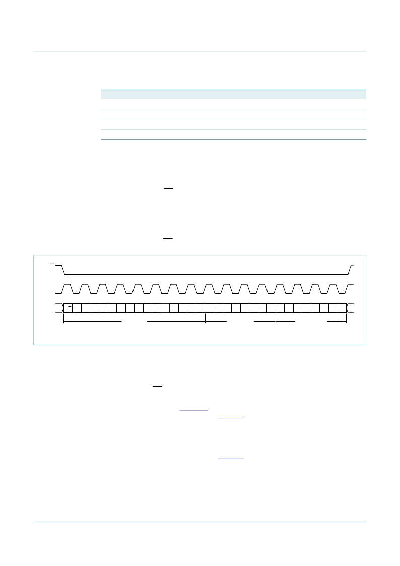
The steps involved in a data transfer are as follows:
1. A falling edge on CS in combination with a rising edge on SCLK determine the start of
communications.
2. The first phase is the transfer of the 2-byte instruction.
3. The second phase is the transfer of the data which can vary in length but is always a
multiple of 8 bits. The MSB is always sent first (for instruction and data bytes).
4. A rising edge on CS indicates the end of data transmission.
11.6.2
Default modes at start-up
During circuit initialization, it does not matter which output data standard has been
selected. At power-up, the device enters Pin control mode.
A falling edge on CS triggers a transition to SPI control mode. When the ADC1115S125
enters SPI control mode, the output data standard (CMOS/LVDS DDR) is determined by
the level on pin SDIO (see
Figure 29
). Once in SPI control mode, the output data standard
can be changed via bit LVDS/CMOS in
Table 23
.
When the ADC1115S125 enters SPI control mode, the output data format (two’s
complement or offset binary) is determined by the level on pin SCLK (gray code can only
be selected via the SPI). Once in SPI control mode, the output data format can be
changed via bit DATA_FORMAT[1:0] in
Table 23
.
Number of data bytes to be transferred after the instruction bytes
W0
Number of bytes transmitted
0
1 byte
1
2 bytes
0
3 bytes
1
4 bytes or more
Fig 28. SPI mode timing
SCLK
SDIO
R/W
W1
W0
A12 A11
A10
A9
A8
A7
A6
A5
A4
A3
A2
A1
A0
D7
D6
D5
D4
D3
D2
D1
D3
D2
D1
D0
D0
D7
D6
D5
D4
Instruction bytes
Register N (data)
Register N + 1 (data)
005aaa062
CS
相關(guān)PDF資料 |
PDF描述 |
|---|---|
| ADC1206S040H | Single 12 bits ADC up to 40 Msps |
| ADC1206S040H | Single 12 bits ADC up to 40 Msps |
| ADC1206S055H | Single 12 bits ADC up to 55 Msps |
| ADC1206S070H | Single 12 bits ADC up to 70 Msps |
| ADC1206S040 | |
相關(guān)代理商/技術(shù)參數(shù) |
參數(shù)描述 |
|---|---|
| ADC1115S125HN/C1 | 制造商:PHILIPS 制造商全稱:NXP Semiconductors 功能描述:Single 11-bit ADC; 125 Msps with input buffer; CMOS or LVDS DDR digital outputs |
| ADC1115S125HN/C1,5 | 功能描述:模數(shù)轉(zhuǎn)換器 - ADC SGL 11b ADC 125MSPS INPUT BUFFER RoHS:否 制造商:Texas Instruments 通道數(shù)量:2 結(jié)構(gòu):Sigma-Delta 轉(zhuǎn)換速率:125 SPs to 8 KSPs 分辨率:24 bit 輸入類型:Differential 信噪比:107 dB 接口類型:SPI 工作電源電壓:1.7 V to 3.6 V, 2.7 V to 5.25 V 最大工作溫度:+ 85 C 安裝風(fēng)格:SMD/SMT 封裝 / 箱體:VQFN-32 |
| ADC1115S125HN-C1 | 功能描述:模數(shù)轉(zhuǎn)換器 - ADC RoHS:否 制造商:Texas Instruments 通道數(shù)量:2 結(jié)構(gòu):Sigma-Delta 轉(zhuǎn)換速率:125 SPs to 8 KSPs 分辨率:24 bit 輸入類型:Differential 信噪比:107 dB 接口類型:SPI 工作電源電壓:1.7 V to 3.6 V, 2.7 V to 5.25 V 最大工作溫度:+ 85 C 安裝風(fēng)格:SMD/SMT 封裝 / 箱體:VQFN-32 |
| ADC1115S125HN-C18 | 制造商:Integrated Device Technology Inc 功能描述:HVQFN40 - Tape and Reel |
發(fā)布緊急采購,3分鐘左右您將得到回復(fù)。