- 您現(xiàn)在的位置:買賣IC網(wǎng) > PDF目錄378283 > ADC12132 (National Semiconductor Corporation) Self-Calibrating 12-Bit Plus Sign Serial I/O A/D Converters with MUX and Sample/Hold PDF資料下載
參數(shù)資料
| 型號(hào): | ADC12132 |
| 廠商: | National Semiconductor Corporation |
| 元件分類: | 串行ADC |
| 英文描述: | Self-Calibrating 12-Bit Plus Sign Serial I/O A/D Converters with MUX and Sample/Hold |
| 中文描述: | 自校準(zhǔn)12位帶符號(hào)串行I /辦公自動(dòng)化/ D轉(zhuǎn)換器MUX和采樣/保持 |
| 文件頁(yè)數(shù): | 28/41頁(yè) |
| 文件大小: | 1085K |
| 代理商: | ADC12132 |
第1頁(yè)第2頁(yè)第3頁(yè)第4頁(yè)第5頁(yè)第6頁(yè)第7頁(yè)第8頁(yè)第9頁(yè)第10頁(yè)第11頁(yè)第12頁(yè)第13頁(yè)第14頁(yè)第15頁(yè)第16頁(yè)第17頁(yè)第18頁(yè)第19頁(yè)第20頁(yè)第21頁(yè)第22頁(yè)第23頁(yè)第24頁(yè)第25頁(yè)第26頁(yè)第27頁(yè)當(dāng)前第28頁(yè)第29頁(yè)第30頁(yè)第31頁(yè)第32頁(yè)第33頁(yè)第34頁(yè)第35頁(yè)第36頁(yè)第37頁(yè)第38頁(yè)第39頁(yè)第40頁(yè)第41頁(yè)
Application Hints
(Continued)
1.3 CS Low Continuously Considerations
When CS is continuously low, it is important to transmit the
exact number of SCLK pulses that the ADC expects. Not do-
ing so will desynchronize the serial communications to the
ADC. When the supply power is first applied to the ADC, it
will expect to see 13 SCLK pulses for each I/O transmission.
The number of SCLK pulses that the ADC expects to see is
the same as the digital output word length. The digital output
word length is controlled by the Data Out (DO) format. The
DO format maybe changed any time a conversion is started
or when the sign bit is turned on or off. The table below de-
tails out the number of clock periods required for different
DO formats:
Number of
SCLKs
Expected
DO Format
12-Bit MSB or LSB First
SIGN OFF
SIGN ON
SIGN OFF
SIGN ON
12
13
16
16-Bit MSB or LSB first
17
If erroneous SCLK pulses desynchronize the communica-
tions, the simplest way to recover is by cycling the power
supply to the device. Not being able to easily resynchronize
the device is a shortcoming of leaving CS low continuously.
The number of clock pulses required for an I/O exchange
may be different for the case when CS is left low continu-
ously vs the case when CS is cycled. Take the I/O sequence
detailed in Figure 7 (Typical Power Supply Sequence) as an
example. The table below lists the number of SCLK pulses
required for each instruction:
Instruction
CS Low
Continuously
13 SCLKs
13 SCLKs
13 SCLKs
13 SCLKs
13 SCLKs
CS Strobed
Auto Cal
Read Status
Read Status
12-Bit + Sign Conv 1
12-Bit + Sign Conv 2
8 SCLKs
8 SCLKs
8 SCLKs
8 SCLKs
13 SCLKs
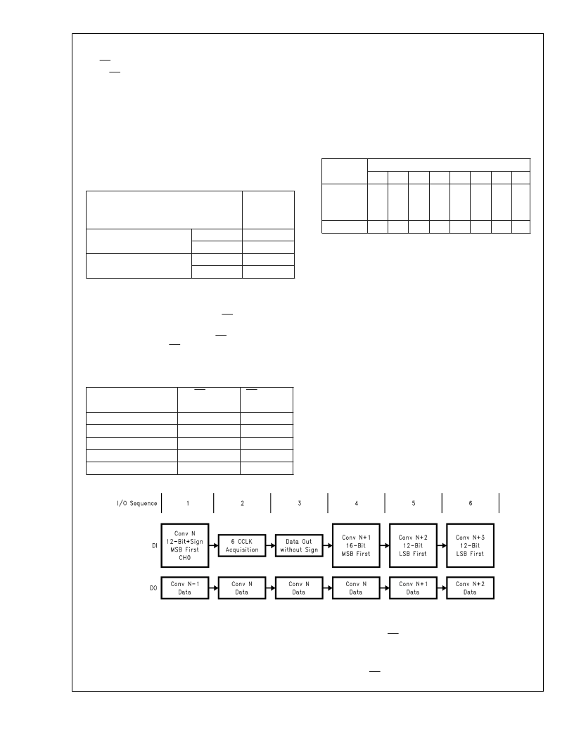
1.4 Analog Input Channel Selection
The data input on DI also selects the channel configuration
for a particular A/D conversion (see Table 2 Table 3 and
Table 4). In Figure 8 the only times when the channel con-
figuration could be modified would be during I/O sequences
1, 4, 5 and 6. Input channels are reselected before the start
of each new conversion. Shown below is the data bit stream
required on DI, during I/O sequence number 4 in Figure 8 to
set CH1 as the positive input and CH0 as the negative input
for the different versions of ADCs:
Part
Number
DI Data
DI3
L
DI0
L
DI1
H
DI2
L
DI4
H
DI5
L
DI6
X
DI7
X
ADC12130
and
ADC12132
ADC12138
L
H
L
L
L
L
H
L
Where X can be a logic high (H) or low (L).
1.5 Power Up/Down
The ADC may be powered down at any time by taking the
PD pin HIGH or by the instruction input on DI (see Table 4
and Table 5 and the Power Up/Down timing diagrams).
When the ADC is powered down in this way, the circuitry
necessary for an A/D conversion is deactivated. The circuitry
necessary for digital I/O is kept active. Hardware power up/
down is controlled by the state of the PD pin. Software
power-up/down is controlled by the instruction issued to the
ADC. If a software power up instruction is issued to the ADC
while a hardware power down is in effect (PD pin high) the
device will remain in the power-down state. If a software
power down instruction is issued to the ADC while a hard-
ware power up is in effect (PD pin low), the device will power
down. When the device is powered down by software, it may
be powered up by either issuing a software power up instruc-
tion or by taking PD pin high and then low. If the power down
command is issued during an A/D conversion, that conver-
sion is disrupted. Therefore, the data output after power up
cannot be relied upon.
1.6 User Mode and Test Mode
An instruction may be issued to the ADC to put it into test
mode. Test mode is used by the manufacturer to verify com-
plete functionality of the device. During test mode CH0–CH7
become active outputs. If the device is inadvertently put into
the test mode with CS continuously low, the serial communi-
cations may be desynchronized. Synchronization may be re-
gained by cycling the power supply voltage to the device.
Cycling the power supply voltage will also set the device into
user mode. If CS is used in the serial interface, theADC may
DS012079-33
FIGURE 8. Changing the ADC’s Conversion Configuration
A
www.national.com
28
相關(guān)PDF資料 |
PDF描述 |
|---|---|
| ADC12138CIWM | 1.2UF/100VDC METAL POLY CAP |
| ADC12132CIMSA | Switch-mode Lead-Acid Battery Charger with User-Selectable Charge Algorithms 16-SOIC -20 to 70 |
| ADC12138 | Self-Calibrating 12-Bit Plus Sign Serial I/O A/D Converters with MUX and Sample/Hold |
| ADC12130CIN | Self-Calibrating 12-Bit Plus Sign Serial I/O A/D Converters with MUX and Sample/Hold |
| ADC12130CIWM | Self-Calibrating 12-Bit Plus Sign Serial I/O A/D Converters with MUX and Sample/Hold |
相關(guān)代理商/技術(shù)參數(shù) |
參數(shù)描述 |
|---|---|
| ADC12132CIMSA | 功能描述:IC ADC 12BIT 20-SSOP RoHS:是 類別:集成電路 (IC) >> 數(shù)據(jù)采集 - 模數(shù)轉(zhuǎn)換器 系列:- 產(chǎn)品培訓(xùn)模塊:Lead (SnPb) Finish for COTS Obsolescence Mitigation Program 標(biāo)準(zhǔn)包裝:2,500 系列:- 位數(shù):12 采樣率(每秒):3M 數(shù)據(jù)接口:- 轉(zhuǎn)換器數(shù)目:- 功率耗散(最大):- 電壓電源:- 工作溫度:- 安裝類型:表面貼裝 封裝/外殼:SOT-23-6 供應(yīng)商設(shè)備封裝:SOT-23-6 包裝:帶卷 (TR) 輸入數(shù)目和類型:- |
| ADC12132CIMSA | 制造商:Texas Instruments 功能描述:IC 12BIT ADC SMD 12132 SSOP20 |
| ADC12132CIMSA/NOPB | 制造商:Texas Instruments 功能描述: |
| ADC12132CIMSAX | 功能描述:IC ADC 12BIT 20-SSOP RoHS:是 類別:集成電路 (IC) >> 數(shù)據(jù)采集 - 模數(shù)轉(zhuǎn)換器 系列:- 產(chǎn)品培訓(xùn)模塊:Lead (SnPb) Finish for COTS Obsolescence Mitigation Program 標(biāo)準(zhǔn)包裝:2,500 系列:- 位數(shù):12 采樣率(每秒):3M 數(shù)據(jù)接口:- 轉(zhuǎn)換器數(shù)目:- 功率耗散(最大):- 電壓電源:- 工作溫度:- 安裝類型:表面貼裝 封裝/外殼:SOT-23-6 供應(yīng)商設(shè)備封裝:SOT-23-6 包裝:帶卷 (TR) 輸入數(shù)目和類型:- |
| ADC12138 | 制造商:NSC 制造商全稱:National Semiconductor 功能描述:Self-Calibrating 12-Bit Plus Sign Serial I/O A/D Converters with MUX and Sample/Hold |
發(fā)布緊急采購(gòu),3分鐘左右您將得到回復(fù)。