- 您現(xiàn)在的位置:買賣IC網(wǎng) > PDF目錄378283 > ADC12138CIMSA (NATIONAL SEMICONDUCTOR CORP) Self-Calibrating 12-Bit Plus Sign Serial I/O A/D Converters with MUX and Sample/Hold PDF資料下載
參數(shù)資料
| 型號: | ADC12138CIMSA |
| 廠商: | NATIONAL SEMICONDUCTOR CORP |
| 元件分類: | ADC |
| 英文描述: | Self-Calibrating 12-Bit Plus Sign Serial I/O A/D Converters with MUX and Sample/Hold |
| 中文描述: | 8-CH 12-BIT SUCCESSIVE APPROXIMATION ADC, SERIAL ACCESS, PDSO28 |
| 封裝: | SSOP-28 |
| 文件頁數(shù): | 34/41頁 |
| 文件大小: | 1085K |
| 代理商: | ADC12138CIMSA |
第1頁第2頁第3頁第4頁第5頁第6頁第7頁第8頁第9頁第10頁第11頁第12頁第13頁第14頁第15頁第16頁第17頁第18頁第19頁第20頁第21頁第22頁第23頁第24頁第25頁第26頁第27頁第28頁第29頁第30頁第31頁第32頁第33頁當前第34頁第35頁第36頁第37頁第38頁第39頁第40頁第41頁
Application Hints
(Continued)
creased to 18 or 34 CCLK periods. For less ADC accuracy
and/or slower CCLK frequencies the S/H’s acquisition time
may be decreased to 6 CCLK periods. To determine the
number of clock periods (N
) required for the acquisition time
with a specific source impedance for the various resolutions
the following equations can be used:
12 Bit + Sign
N
C
= [R
S
+ 2.3] x f
CK
x 0.824
Where f
CK
is the conversion clock (CCLK) frequency in MHz
and R
. As an ex-
ample, operating with a resolution of 12 Bits+sign, a 5 MHz
clock frequency and maximum acquistion time of 34 conver-
sion clock periods the ADC’s analog inputs can handle a
source impedance as high as 6 k
. The acquisition time may
also be extended to compensate for the settling or response
time of external circuitry connected between the MUXOUT
and A/DIN pins.
The acquisition time t
is started by a falling edge of SCLK
and ended by a rising edge of CCLK (see timing diagrams).
If SCLK and CCLK are asynchronous one extra CCLK clock
period may be inserted into the programmed acquisition time
for synchronization. Therefore with asnychronous SCLK and
CCLKs the acquisition time will change from conversion to
conversion.
7.0 INPUT BYPASS CAPACITANCE
External capacitors (0.01 μF–0.1 μF) can be connected be-
tween the analog input pins, CH0–CH7, and analog ground
to filter any noise caused by inductive pickup associated with
long input leads. These capacitors will not degrade the con-
version accuracy.
8.0 NOISE
The leads to each of the analog multiplexer input pins should
be kept as short as possible. This will minimize input noise
and clock frequency coupling that can cause conversion er-
rors. Input filtering can be used to reduce the effects of the
noise sources.
9.0 POWER SUPPLIES
Noise spikes on the V
A+
and V
D+
supply lines can cause
conversion errors; the comparator will respond to the noise.
The ADC is especially sensitive to any power supply spikes
that occur during the auto-zero or linearity correction. The
minimum power supply bypassing capacitors recommended
are low inductance tantalum capacitors of 10 μF or greater
paralleled with 0.1 μF monolithic ceramic capacitors. More or
different bypassing may be necessary depending on the
overall system requirements. Separate bypass capacitors
should be used for the V
A+
and V
D+
supplies and placed as
close as possible to these pins.
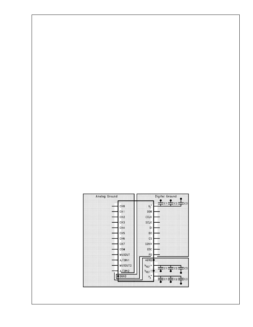
10.0 GROUNDING
The ADC12130/2/8’s
through proper grounding techniques. These include the use
of separate analog and digital ground planes. The digital
ground plane is placed under all components that handle
digital signals, while the analog ground plane is placed under
all components that handle analog signals. The digital and
analog ground planes are connected together at only one
point, either the power supply ground or at the pins of the
ADC. This greatly reduces the occurence of ground loops
and noise.
Shown in Figure 18 is the ideal ground plane layout for the
ADC12138 along with ideal placement of the bypass capaci-
tors. The circuit board layout shown in Figure 18 uses three
bypass capacitors: 0.01 μF (C1) and 0.1 μF (C2) surface
mount capacitors and 10 μF (C3) tantalum capacitor.
performance
can
be
maximized
DS012079-45
FIGURE 18. Ideal Ground Plane
A
www.national.com
34
相關PDF資料 |
PDF描述 |
|---|---|
| ADC12138CIN | Self-Calibrating 12-Bit Plus Sign Serial I/O A/D Converters with MUX and Sample/Hold |
| ADC12181 | 12-Bit, 10 MHz Self-Calibrating, Pipelined A/D Converter with Internal Sample & Hold |
| ADC12181CIVT | 12-Bit, 10 MHz Self-Calibrating, Pipelined A/D Converter with Internal Sample & Hold |
| ADC12181EVAL | 12-Bit, 5 MHz Self-Calibrating, Pipelined A/D Converter |
| ADC12191CIVT | 12-Bit, 10 MHz Self-Calibrating, Pipelined A/D Converter with Internal Sample & Hold |
相關代理商/技術參數(shù) |
參數(shù)描述 |
|---|---|
| ADC12138CIMSA/NOPB | 功能描述:模數(shù)轉(zhuǎn)換器 - ADC SELF-CALIBR 12B PLUS SIGN SERIAL I/O ADC RoHS:否 制造商:Texas Instruments 通道數(shù)量:2 結(jié)構(gòu):Sigma-Delta 轉(zhuǎn)換速率:125 SPs to 8 KSPs 分辨率:24 bit 輸入類型:Differential 信噪比:107 dB 接口類型:SPI 工作電源電壓:1.7 V to 3.6 V, 2.7 V to 5.25 V 最大工作溫度:+ 85 C 安裝風格:SMD/SMT 封裝 / 箱體:VQFN-32 |
| ADC12138CIMSANOPB | 制造商:TI 功能描述:Pb Free |
| ADC12138CIMSAX | 功能描述:模數(shù)轉(zhuǎn)換器 - ADC RoHS:否 制造商:Texas Instruments 通道數(shù)量:2 結(jié)構(gòu):Sigma-Delta 轉(zhuǎn)換速率:125 SPs to 8 KSPs 分辨率:24 bit 輸入類型:Differential 信噪比:107 dB 接口類型:SPI 工作電源電壓:1.7 V to 3.6 V, 2.7 V to 5.25 V 最大工作溫度:+ 85 C 安裝風格:SMD/SMT 封裝 / 箱體:VQFN-32 |
| ADC12138CIMSAX/NOPB | 功能描述:模數(shù)轉(zhuǎn)換器 - ADC RoHS:否 制造商:Texas Instruments 通道數(shù)量:2 結(jié)構(gòu):Sigma-Delta 轉(zhuǎn)換速率:125 SPs to 8 KSPs 分辨率:24 bit 輸入類型:Differential 信噪比:107 dB 接口類型:SPI 工作電源電壓:1.7 V to 3.6 V, 2.7 V to 5.25 V 最大工作溫度:+ 85 C 安裝風格:SMD/SMT 封裝 / 箱體:VQFN-32 |
| ADC12138CIN | 制造商:Texas Instruments 功能描述:IC 12BIT ADC 12138 DIP28 |
發(fā)布緊急采購,3分鐘左右您將得到回復。