- 您現(xiàn)在的位置:買賣IC網(wǎng) > PDF目錄378283 > ADC121S101CIMFX (NATIONAL SEMICONDUCTOR CORP) 1MSPS, 12-/10-/8-Bit A/D Converters in SOT-23 PDF資料下載
參數(shù)資料
| 型號: | ADC121S101CIMFX |
| 廠商: | NATIONAL SEMICONDUCTOR CORP |
| 元件分類: | ADC |
| 英文描述: | 1MSPS, 12-/10-/8-Bit A/D Converters in SOT-23 |
| 中文描述: | 1-CH 12-BIT SUCCESSIVE APPROXIMATION ADC, SERIAL ACCESS, PDSO6 |
| 封裝: | SOT-23, 6 PIN |
| 文件頁數(shù): | 5/20頁 |
| 文件大小: | 1049K |
| 代理商: | ADC121S101CIMFX |
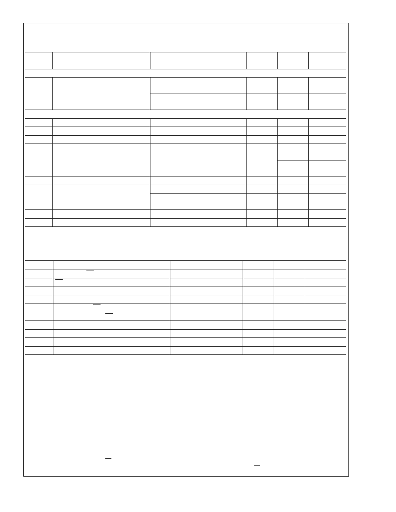
ADC121S625 Converter Electrical Characteristics
(Note 8) (Continued)
The following specifications apply for V
= +4.5V to 5.5V, V
= 2.5V, f
= 0.8 to 3.2 MHz, f
IN
= 20 kHz, C
L
= 100 pF, un-
less otherwise noted.
Boldface limits apply for T
A
= T
MIN
to T
MAX
: all other limits T
A
= 25C.
Symbol
Parameter
Conditions
Typical
Limits
Units
(Note 7)
POWER SUPPLY CHARACTERISTICS
PSRR
Power Supply Rejection Ratio
Offset Change with 1.0V change in
V
A
Gain Error Change with 1.0V change
in V
A
71
dB
83
dB
AC ELECTRICAL CHARACTERISTICS
f
SCLK
Maximum Clock Frequency
f
SCLK
Minimum Clock Frequency
f
S
Maximum Sample Rate
4.8
200
300
3.2
800
200
MHz (min)
kHz (max)
ksps (min)
SCLK cycles
(min)
SCLK cycles
(max)
SCLK cycles
SCLK cycles
SCLK cycles
(min)
ksps (max)
ns
t
ACQ
Track/Hold Acquisition Time
1.5
2.0
t
CONV
Conversion Time
12
12
16
t
CYC
Throughput Time
Normal Operation
Short Cycled
14
f
RATE
t
AD
Throughput Rate
Aperture Delay
200
6
ADC121S625 Timing Specifications
(Note 8)
The following specifications apply for V
A
= +4.5V to 5.5V, V
REF
= 2.5V, f
SCLK
= 0.8 MHz to 3.2 MHz, C
L
= 100 pF,
Boldface
limits apply for T
A
= T
MIN
to T
MAX
: all other limits T
A
= 25C.
Symbol
Parameter
t
CFCS
SCLK Fall toCS Fall
t
CSCR
CS Fall to SCLK Rise
(Note 9)
t
CHLD
SCLK Fall to Data Change Hold Time
(Note 9)
t
CDV
SCLK Fall to Next D
OUT
Valid
t
DIS
Rising Edge of CS To D
OUT
Disabled
t
EN
2nd SCLK Fall after CS Fall to D
OUT
Enabled
t
CH
SCLK High Time
t
CL
SCLK Low Time
t
r
D
OUT
Rise Time
t
f
D
OUT Fall Time
Conditions
Typical
Limits
0
0
10
100
50
50
60
60
50
50
Units
ns (min)
ns (min)
ns (min)
ns (max)
ns (max)
ns (max)
ns (min)
ns (min)
ns (max)
ns (max)
38
38
6
42
42
5
13
Note 1:
Absolute maximum ratings are limiting values which indicate limits beyond which damage to the device may occur. Operating Ratings indicate conditions
for which the device is functional, but do not guarantee specific performance limits. For guaranteed specifications and test conditions, see the Electrical
Characteristics. The guaranteed specifications apply only for the test conditions listed. Some performance characteristics may degrade when the device is not
operated under the listed test conditions.
Note 2:
All voltages are measured with respect to GND = 0V, unless otherwise specified.
Note 3:
When the input voltage at any pin exceeds the power supplies (that is, V
IN
<
AGND or V
IN
>
V
A
or V
D
), the current at that pin should be limited to 10 mA.
The 50 mA maximum package input current rating limits the number of pins that can safely exceed the power supplies with an input current of 10 mA to five.
Note 4:
The absolute maximum junction temperature (T
J
max) for this device is 150C. The maximum allowable power dissipation is dictated by T
J
max, the
junction-to-ambient thermal resistance (
θ
JA
), and the ambient temperature (T
A
), and can be calculated using the formula P
D
MAX = (T
J
max T
A
)/
θ
JA
. The values
for maximum power dissipation listed above will be reached only when the ADC121S625 is operated in a severe fault condition (e.g. when input or output pins are
driven beyond the power supply voltages, or the power supply polarity is reversed). Obviously, such conditions should always be avoided.
Note 5:
Human body model is 100 pF capacitor discharged through a 1.5 k
resistor. Machine model is 220 pF discharged through ZERO ohms.
Note 6:
See AN450, “Surface Mounting Methods and Their Effect on Product Reliability”, or the section entitled “Surface Mount” found in any post 1986 National
Semiconductor Linear Data Book, for other methods of soldering surface mount devices.
Note 7:
Tested limits are guaranteed to National’s AOQL (Average Outgoing Quality Level).
Note 8:
Data sheet min/max specification limits are guaranteed by design, test, or statistical analysis.
Note 9:
Clock should be in low when CS is asserted, as indicated by the t
CSCR
and t
CFCS
specifications.
Note 10:
While the maximum sample rate is f
SCLK
/16, the actual sample rate may be lower than this by having the CS rate being slower than f
SCLK
/16.
A
www.national.com
5
相關PDF資料 |
PDF描述 |
|---|---|
| ADC121S101CIMF | 1MSPS, 12-/10-/8-Bit A/D Converters in SOT-23 |
| ADC121S625CIMMX | 12-Bit, 50 ksps to 200 ksps, Differential Input, Micro Power Sampling A/D Converter |
| ADC121S625EVAL | 12-Bit, 50 ksps to 200 ksps, Differential Input, Micro Power Sampling A/D Converter |
| ADC121S101EVAL | 1MSPS, 12-/10-/8-Bit A/D Converters in SOT-23 |
| ADC12281CIVT | 12-Bit, 20 MSPS Single-Ended Input, Pipelined A/D Converter |
相關代理商/技術參數(shù) |
參數(shù)描述 |
|---|---|
| ADC121S101CIMFX/NOPB | 功能描述:模數(shù)轉換器 - ADC RoHS:否 制造商:Texas Instruments 通道數(shù)量:2 結構:Sigma-Delta 轉換速率:125 SPs to 8 KSPs 分辨率:24 bit 輸入類型:Differential 信噪比:107 dB 接口類型:SPI 工作電源電壓:1.7 V to 3.6 V, 2.7 V to 5.25 V 最大工作溫度:+ 85 C 安裝風格:SMD/SMT 封裝 / 箱體:VQFN-32 |
| ADC121S101CISD | 功能描述:模數(shù)轉換器 - ADC RoHS:否 制造商:Texas Instruments 通道數(shù)量:2 結構:Sigma-Delta 轉換速率:125 SPs to 8 KSPs 分辨率:24 bit 輸入類型:Differential 信噪比:107 dB 接口類型:SPI 工作電源電壓:1.7 V to 3.6 V, 2.7 V to 5.25 V 最大工作溫度:+ 85 C 安裝風格:SMD/SMT 封裝 / 箱體:VQFN-32 |
| ADC121S101CISD/NOPB | 功能描述:模數(shù)轉換器 - ADC RoHS:否 制造商:Texas Instruments 通道數(shù)量:2 結構:Sigma-Delta 轉換速率:125 SPs to 8 KSPs 分辨率:24 bit 輸入類型:Differential 信噪比:107 dB 接口類型:SPI 工作電源電壓:1.7 V to 3.6 V, 2.7 V to 5.25 V 最大工作溫度:+ 85 C 安裝風格:SMD/SMT 封裝 / 箱體:VQFN-32 |
| ADC121S101CISDX | 功能描述:模數(shù)轉換器 - ADC RoHS:否 制造商:Texas Instruments 通道數(shù)量:2 結構:Sigma-Delta 轉換速率:125 SPs to 8 KSPs 分辨率:24 bit 輸入類型:Differential 信噪比:107 dB 接口類型:SPI 工作電源電壓:1.7 V to 3.6 V, 2.7 V to 5.25 V 最大工作溫度:+ 85 C 安裝風格:SMD/SMT 封裝 / 箱體:VQFN-32 |
| ADC121S101CISDX/NOPB | 功能描述:模數(shù)轉換器 - ADC RoHS:否 制造商:Texas Instruments 通道數(shù)量:2 結構:Sigma-Delta 轉換速率:125 SPs to 8 KSPs 分辨率:24 bit 輸入類型:Differential 信噪比:107 dB 接口類型:SPI 工作電源電壓:1.7 V to 3.6 V, 2.7 V to 5.25 V 最大工作溫度:+ 85 C 安裝風格:SMD/SMT 封裝 / 箱體:VQFN-32 |
發(fā)布緊急采購,3分鐘左右您將得到回復。