- 您現(xiàn)在的位置:買賣IC網(wǎng) > PDF目錄378284 > ADC1251CIJ (NATIONAL SEMICONDUCTOR CORP) Self-Calibrating 12-Bit Plus Sign A/D Converter with Sample-and-Hold PDF資料下載
參數(shù)資料
| 型號(hào): | ADC1251CIJ |
| 廠商: | NATIONAL SEMICONDUCTOR CORP |
| 元件分類: | ADC |
| 英文描述: | Self-Calibrating 12-Bit Plus Sign A/D Converter with Sample-and-Hold |
| 中文描述: | 1-CH 12-BIT SUCCESSIVE APPROXIMATION ADC, PARALLEL ACCESS, CDIP24 |
| 封裝: | CERAMIC, DIP-24 |
| 文件頁數(shù): | 13/16頁 |
| 文件大?。?/td> | 301K |
| 代理商: | ADC1251CIJ |
3.0 Analog Considerations
(Continued)
*
Tantalum
**
Ceramic
TL/H/11024–20
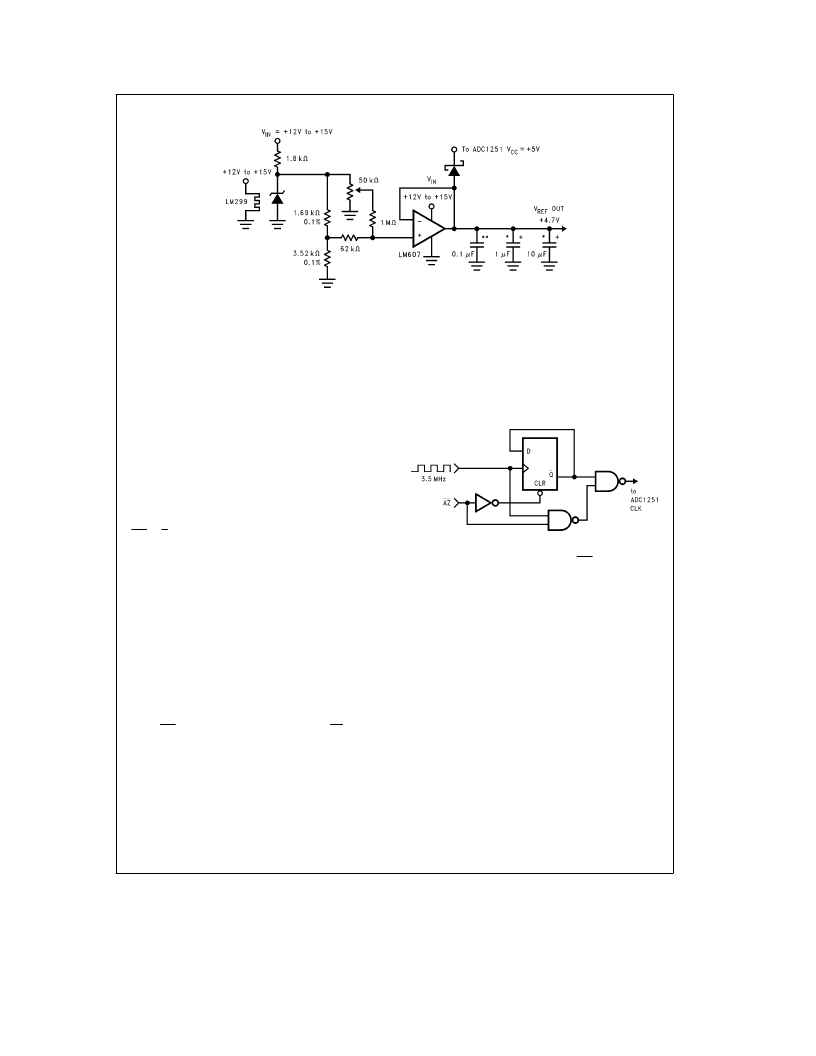
FIGURE 4. Low Drift Extremely Stable Reference Circuit
In a ratiometric system, the analog input voltage is propor-
tional to the voltage used for the A/D reference. When this
voltage is the system power supply, the V
REF
pin can be
tied to V
CC
. This technique relaxes the stability requirement
of the system reference as the analog input and A/D refer-
ence move together maintaining the same output code for a
given input condition.
For absolute accuracy, where the analog input varies be-
tween very specific voltage limits, the reference pin can be
biased with a time and temperature stable voltage source.
In general, the magnitude of the reference voltage will re-
quire an initial adjustment to null out full-scale errors.
3.2 ACQUISITION WINDOW
As shown in the timing diagrams there are three different
methods of starting a conversion, each of which affects the
acquisition window and timing.
With Auto-Zero high a conversion can be started with the
WR or S/H controls. In either method of starting a conver-
sion the rising edge of EOC signals the actual beginning of
the acquisition window. At this time a voltage spike may be
noticed on the analog input of the ADC1251 whose ampli-
tude is dependent on the input voltage and the source re-
sistance. The timing diagrams for these two methods of
starting a conversion do not show the acquisition window
starting at this time because the acquisition time (t
A
) must
start after the conversion result high and low bytes have
been read. This is necessary since activating and deactivat-
ing the digital outputs (DB0/DB7–DB8/DB12) causes cur-
rent fluctuations in the ADC1251’s internal DV
CC
lines. This
generates digital noise which couples into the capacitive
ladder that stores the analog input voltage. Therefore, the
time interval between the rising edge of EOC and the sec-
ond read is inappropriate for analog input voltage acquisi-
tion.
When WR is used to start a conversion with AZ low the
Auto-Zero cycle is inserted before the acquisition window. In
this method the acquisition window is internally controlled
by the ADC1251 and lasts for approximately 7 clock peri-
ods. Since the acquisition window needs to be at least
3.5
m
s at all times, when using Auto-Zero the maximum
clock frequency is limited to 2 MHz. The zero error with the
Auto-Zero cycle is production tested at a clock frequency of
1.75 MHz. This accommodates easy switching between a
conversion with the Auto-Zero cycle (f
CLK
e
1.75 MHz) and
without (f
CLK
e
3.5 MHz) as shown in Figure 5.
TL/H/11024–21
FIGURE 5. Switching between a Conversion with and
without Auto-Zero when Using WR Control
3.3 INPUT CURRENT
Because the input network of the ADC1251 is made up of a
switch and a network of capacitors a charging current will
flow into or out of (depending on the input voltage polarity)
the analog input pin (V
IN
) on the start of the analog input
sampling period. The peak value of this current will depend
on the actual input voltage applied and the source resist-
ance.
3.4 NOISE
The leads to the analog input pin should be kept as short as
possible to minimize input noise coupling. Both noise and
undesired digital clock coupling to this input can cause er-
rors. Input filtering can be used to reduce the effects of
these noise sources.
13
相關(guān)PDF資料 |
PDF描述 |
|---|---|
| ADC12662CIVF | 12-Bit, 1.5 MHz, 200 mW A/D Converter with Input Multiplexer and Sample/Hold |
| ADC12662 | 12-Bit, 1.5 MHz, 200 mW A/D Converter with Input Multiplexer and Sample/Hold |
| ADC12662CIV | 12-Bit, 1.5 MHz, 200 mW A/D Converter with Input Multiplexer and Sample/Hold |
| ADC12762 | 12-Bit, 1.4 MHz, 300 mW A/D Converter with Input Multiplexer and Sample/Hold |
| ADC12762CCV | Low Dropout Linear 1-cell Li-Ion Charge Controller with AutoCompTM, 4.2V 8-MSOP -20 to 70 |
相關(guān)代理商/技術(shù)參數(shù) |
參數(shù)描述 |
|---|---|
| ADC1251CMJ | 制造商:NSC 制造商全稱:National Semiconductor 功能描述:Self-Calibrating 12-Bit Plus Sign A/D Converter with Sample-and-Hold |
| ADC1251CMJ/883 | 制造商:NSC 制造商全稱:National Semiconductor 功能描述:Self-Calibrating 12-Bit Plus Sign A/D Converter with Sample-and-Hold |
| ADC1255X | 制造商:未知廠家 制造商全稱:未知廠家 功能描述:ADC1255X 10-Bit 250KSPS SAR ADC|Data Sheet |
| ADC1256X | 制造商:未知廠家 制造商全稱:未知廠家 功能描述:ADC1256X 12-Bit 20MSPS ADC|Data Sheet |
| ADC126 | 制造商:MPSIND 制造商全稱:MPS Industries, Inc. 功能描述:1W, Miniature SIP, Single & Dual Output DC/DC Converters |
發(fā)布緊急采購,3分鐘左右您將得到回復(fù)。