- 您現(xiàn)在的位置:買賣IC網(wǎng) > PDF目錄362157 > AFL2828SZ DC to DC Converter PDF資料下載
參數(shù)資料
| 型號(hào): | AFL2828SZ |
| 英文描述: | DC to DC Converter |
| 中文描述: | DC至DC轉(zhuǎn)換器 |
| 文件頁數(shù): | 9/11頁 |
| 文件大?。?/td> | 115K |
| 代理商: | AFL2828SZ |
www.irf.com
9
AFL28XXS Series
Table 1. Nominal Resistance of Cu Wire
Wire Size, AWG
Resistance per ft
24 Ga
22 Ga
20 Ga
18 Ga
16 Ga
14 Ga
12 Ga
25.7 m
16.2 m
10.1 m
6.4 m
4.0 m
2.5 m
1.6 m
Incorporation of a 100 μfd capacitor at the input terminals
is recommended as compensation for the dynamic ef-
fects of the parasitic resistance of the input cable reacting
with the complex impedance of the converter input, and to
provide an energy reservoir for transient input current
requirements.
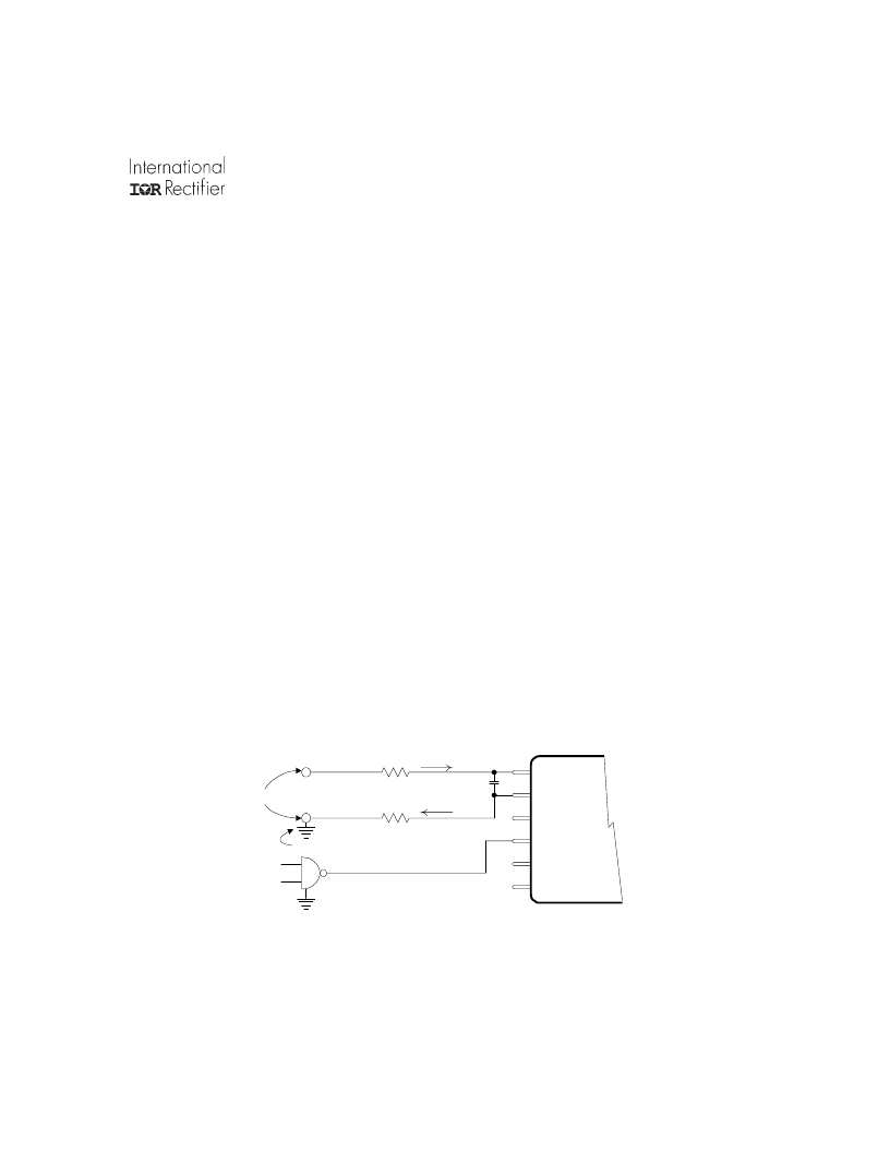
Figure VI. Problems of Parasitic Resistance in input Leads
(See text)
Vin
Rtn
Case
Enable 1
Sync Out
Sync In
R
p
R
p
I
R tn
I
in
e
source
System Ground
e
R tn
100
μfd
As an example of the effects of parasitic resistance, con-
sider an AFL2815S operating at full power of 120 W. From
the specification sheet, this device has a minimum effi-
ciency of 83% which represents an input power of more
than 145 W. If we consider the case where line voltage is at
its’ minimum of 16 volts, the steady state input current
necessary for this example will be slightly greater than 9
amperes. If this device were connected to a voltage source
with 10 feet of 20 gauge wire, the round trip (input and
return) would result in 0.2
of resistance and 1.8 volts of
drop from the source to the converter. To assure 16 volts
at the input, a source closer to 18 volts would be required.
In applications using the paralleling option, this drop will be
multiplied by the number of paralleled devices. By choosing
14 or 16 gauge wire in this example, the parasitic resis-
tance and resulting voltage drop will be reduced to 25% or
31% of that with 20 gauge wire.
Another potential problem resulting from parasitically in-
duced voltage drop on the input lines is with regard to the
operation of the enable 1 port. The minimum and maxi-
mum operating levels required to operate this port are
specified with respect to the input common return line at
the converter. If a logic signal is generated with respect to
a ‘common’ that is distant from the converter, the effects of
the voltage drop over the return line must be considered
when establishing the worst case TTL switching levels.
These drops will effectively impart a shift to the logic lev-
els. In Figure VI, it can be seen that referred to system
ground, the voltage on the input return pin is given by
e
Rtn
= I
Rtn
R
P
Therefore, the logic signal level generated in the system
must be capable of a TTL logic high plus sufficient addi-
tional amplitude to overcome e
. When the converter is
inhibited, I
diminishes to near zero and e
Rtn
will then be at
system ground.
相關(guān)PDF資料 |
PDF描述 |
|---|---|
| AFL2812SZ | DC to DC Converter |
| AFL2815D | Hi-Rel DC-DC Standard Dual Converter in a AFL package |
| AG-40 | GLAND M40 22-32MM |
| AG-50 | GLAND M50 30-38MM |
| AG-63 | GLAND M63 34-44MM |
相關(guān)代理商/技術(shù)參數(shù) |
參數(shù)描述 |
|---|---|
| AFL2828SZ/CH | 制造商:未知廠家 制造商全稱:未知廠家 功能描述:DC to DC Converter |
| AFL2828SZ/ES | 制造商:International Rectifier 功能描述:DC/DC CONVERTER, ENVIRONMENTAL SCREENING - Bulk |
| AFL2828SZ/HB | 制造商:International Rectifier 功能描述:DC/DC CONVERTER, CLASS H EQUIVALENT, NO ELEM EVAL - Bulk |
| AFL2828SZ-CH | 制造商:IRF 制造商全稱:International Rectifier 功能描述:ADVANCED ANALOG HIGH RELIABILITY HYBRID DC/DC CONVERTERS |
| AFL2828SZ-ES | 制造商:IRF 制造商全稱:International Rectifier 功能描述:ADVANCED ANALOG HIGH RELIABILITY HYBRID DC/DC CONVERTERS |
發(fā)布緊急采購(gòu),3分鐘左右您將得到回復(fù)。