- 您現(xiàn)在的位置:買賣IC網(wǎng) > PDF目錄166093 > AFL5015DY/ESPBF 2-OUTPUT 100 W DC-DC REG PWR SUPPLY MODULE PDF資料下載
參數(shù)資料
| 型號: | AFL5015DY/ESPBF |
| 元件分類: | 電源模塊 |
| 英文描述: | 2-OUTPUT 100 W DC-DC REG PWR SUPPLY MODULE |
| 封裝: | 0.380 INCH, LOW PROFILE, SEAM WELDED PACKAGE-12 |
| 文件頁數(shù): | 6/10頁 |
| 文件大小: | 82K |
| 代理商: | AFL5015DY/ESPBF |

www.irf.com
5
AFL50XXD Series
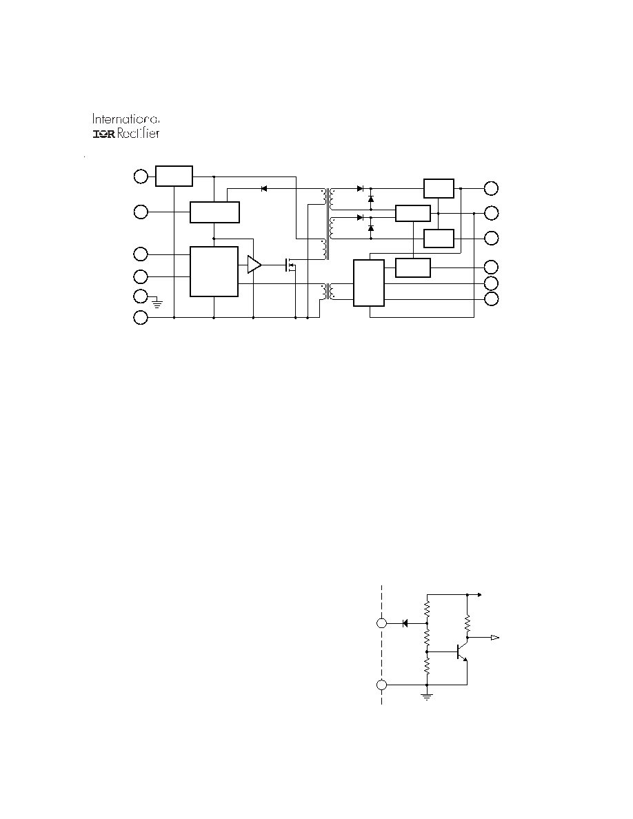
AFL50XXD Circuit Description
Figure I. AFL Dual Output Block Diagram
Figure II. Enable Input Equivalent Circuit
Circuit Operation and Application Information
Inhibiting Converter Output
As an alternative to application and removal of the DC volt-
age to the input, the user can control the converter output
by providing TTL compatible, positive logic signals to either
of two enable pins (pin 4 or 12). The distinction between
these two signal ports is that enable 1 (pin 4) is referenced
to the input return (pin 2) while enable 2 (pin 12) is refer-
enced to the output return (pin 8). Thus, the user has
access to an inhibit function on either side of the isolation
barrier. Each port is internally pulled “high” so that when not
used, an open connection on both enable pins permits nor-
mal converter operation. When their use is desired, a logi-
cal “l(fā)ow” on either port will shut the converter down.
ERROR
AMP
& REF
OUTPUT
FILTER
INPUT
FILTER
OUTPUT RETURN
DC INPUT
INPUT RETURN
FB
CONTROL
1
2
4
3
5
6
SYNC INPUT
CURRENT
SENSE
ENABLE 2
SHARE
AMPLIFIER
7
11
10
9
12
8
+ OUTPUT
SYNC OUTPUT
ENABLE 1
CASE
PRIMARY
BIAS SUPPLY
- OUTPUT
TRIM
FILTER
OUTPUT
The AFL series of converters employ a forward switched
mode converter topology. (refer to Figure I.) Operation of
the device is initiated when a DC voltage whose magnitude
is within the specified input limits is applied between pins 1
and 2. If pins 4 and 12 are enabled (at a logical 1 or open)
the primary bias supply will begin generating a regulated
housekeeping voltage bringing the circuitry on the primary
side of the converter to life. Two power MOSFETs used to
chop the DC input voltage into a high frequency square
wave, apply this chopped voltage to the power transformer.
As this switching is initiated, a voltage is impressed on a
second winding of the power transformer which is then
rectified and applied to the primary bias supply. When this
occurs, the input voltage is excluded from the bias voltage
generator and the primary bias voltage becomes internally
generated.
The switched voltage impressed on the secondary output
transformer windings is rectified and filtered to provide the
positive and negative converter output voltages. An error
amplifier on the secondary side compares the positive out-
put voltage to a precision reference and generates an error
signal proportional to the difference. This error signal is
magnetically coupled through the feedback transformer into
the control section of the converter varying the pulse width
of the square wave signal driving the MOSFETs, narrowing
the pulse width if the output voltage is too high and widen-
ing it if it is too low. These pulse width variations provide
the necessary corrections to maintain the magnitude of
output voltage within its’ specified limits.
Because the primary and secondary sides are coupled by
magnetic elements, full isolation from input to output is
achieved.
ancillary features, basic operation of the AFL50XXD series
can be initiated by simply applying an input voltage to pins 1
and 2 and connecting the appropriate loads between pins
7, 8, and 9. Of course, operation of anyconverter with high
power density should not be attempted before secure at-
tachment to an appropriate heat dissipator. (See Thermal
Considerations, page 7)
Although incorporating several sophisticated and useful
D isable
100K
290K
180K
1N 4148
2N 3904
+ 5 .6 V
P in 4 or
P in 12
P in 2 or
Pin 8
相關(guān)PDF資料 |
PDF描述 |
|---|---|
| AFT20012 | 6000 MHz - 20000 MHz RF/MICROWAVE WIDE BAND LOW POWER AMPLIFIER |
| AG303-63G | 0 MHz - 6000 MHz RF/MICROWAVE WIDE BAND LOW POWER AMPLIFIER |
| AGA20BP | ELECTRIC FUSE, 20A, 32VAC, 32VDC, INLINE/HOLDER |
| AGA15BP | ELECTRIC FUSE, 15A, 32VAC, 32VDC, INLINE/HOLDER |
| AGA2BP | ELECTRIC FUSE, 2A, 32VAC, 32VDC, INLINE/HOLDER |
相關(guān)代理商/技術(shù)參數(shù) |
參數(shù)描述 |
|---|---|
| AFL5015DY-HB | 制造商:IRF 制造商全稱:International Rectifier 功能描述:ADVANCED ANALOG HIGH RELIABILITY HYBRID DC/DC CONVERTERS |
| AFL5015DZ | 制造商:International Rectifier 功能描述:DC/DC CONVERTER, MINIMUM SCREENING - Bulk |
| AFL5015DZ/CH | 制造商:International Rectifier 功能描述:DC/DC CONVERTER, CLASS H - Bulk |
| AFL5015DZ/ES | 制造商:International Rectifier 功能描述:DC/DC CONVERTER, ENVIRONMENTAL SCREENING - Bulk |
| AFL5015DZ/HB | 制造商:International Rectifier 功能描述:DC/DC CONVERTER, CLASS H EQUIVALENT, NO ELEM EVAL - Bulk |
發(fā)布緊急采購,3分鐘左右您將得到回復。