- 您現(xiàn)在的位置:買賣IC網(wǎng) > PDF目錄42888 > AGR09090EF UHF BAND, Si, N-CHANNEL, RF POWER, MOSFET PDF資料下載
參數(shù)資料
| 型號: | AGR09090EF |
| 元件分類: | 功率晶體管 |
| 英文描述: | UHF BAND, Si, N-CHANNEL, RF POWER, MOSFET |
| 封裝: | FM-2 |
| 文件頁數(shù): | 1/15頁 |
| 文件大小: | 661K |
| 代理商: | AGR09090EF |
Preliminary Data Sheet
April 2004
AGR09090EF
90 W, 865 MHz—960 MHz, N-Channel E-Mode, Lateral MOSFET
Introduction
The
AGR09090EF is a high-voltage, gold-metalized, lat-
erally diffused metal oxide semiconductor (LDMOS) RF
power transistor suitable for global system for mobile com-
munication (GSM), enhanced data for global evolution
(EDGE), cellular, and multicarrier class AB power amplifier
applications. This device is manufactured on an advanced
LDMOS technology, offering state-of-the-art performance
and reliability. Packaged in an industry-standard package
and capable of delivering a minimum output power of 90 W,
it is ideally suited for today's wireless base station RF
power amplifier applications.
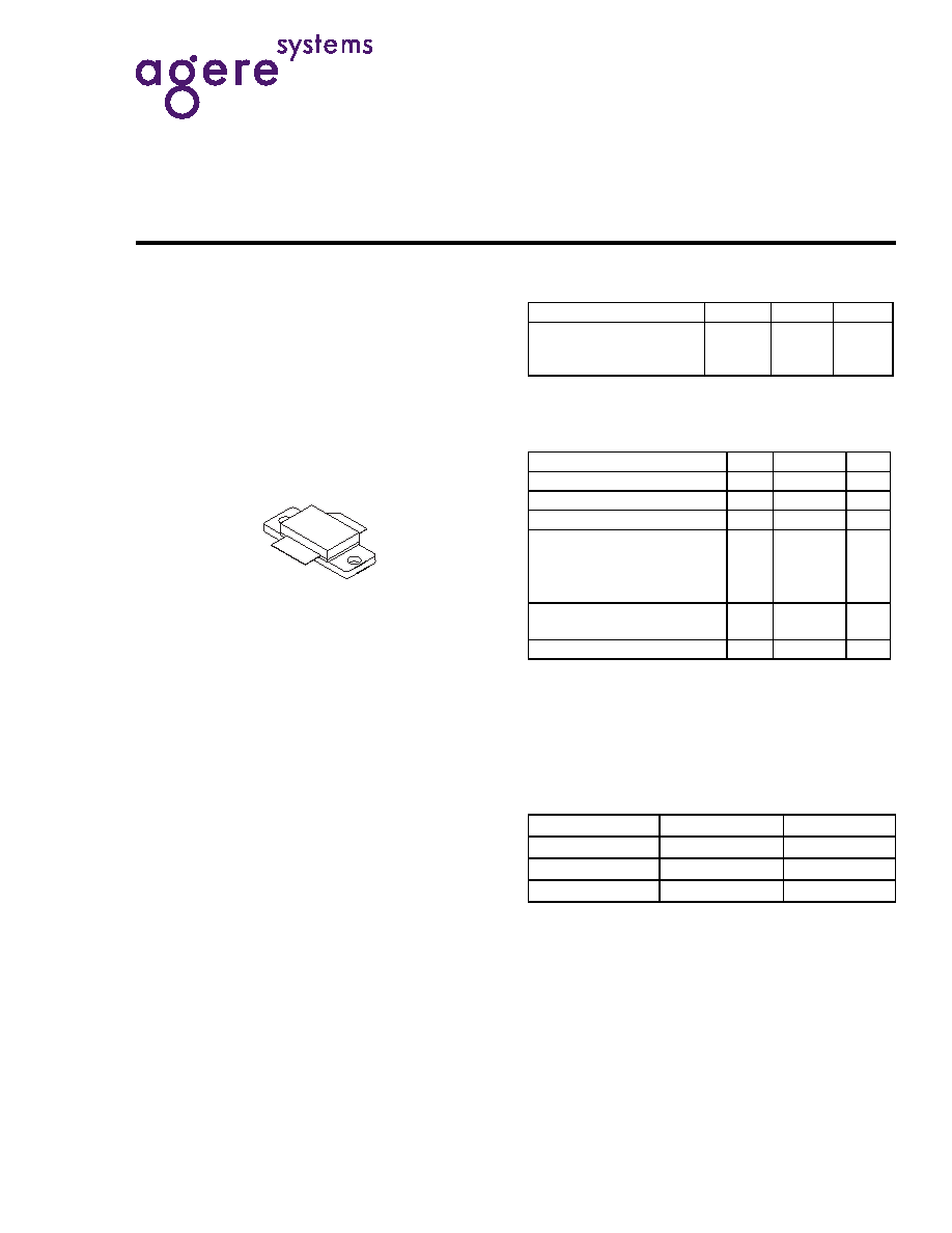
Figure 1. AGR09090EF (Flanged) Package
GSM Features
I Typical performance ratings for GSM EDGE
(f = 941 MHz, POUT = 40 W):
— Modulation spectrum:
@ ±400 kHz = –60 dBc.
@ ±600 kHz = –72 dBc.
— Error vector magnitude (EVM) = 2.3%.
I Typical performance over entire GSM band:
— P1dB: 105 W typical.
— Power gain: @ P1dB = 17.8 dB.
— Efficiency @ P1dB = 60% typical.
— Return loss: –10 dB.
Cellular Features
I Typical performance ratings (f = 880 MHz,
POUT = 40 W):
— Modulation spectrum:
@ ±400 kHz = –60 dBc.
@ ±600 kHz = –72 dBc.
— Error vector magnitude (EVM) = 2.3%.
I Typical performance over entire GSM band:
— P1dB: 105 W typical.
— Power gain: @ P1dB = 17.6 dB.
— Efficiency @ P1dB = 60% typical.
— Return loss: –10 dB.
GSM/Cellular Features
I High-reliability, gold-metalization process.
I Internally matched.
I High gain, efficiency, and linearity.
I Integrated ESD protection.
I 90 W minimum output power.
Table 1. Thermal Characteristics
(921 MHz—960 MHz, and 865 MHz—895 MHz)
Table 2. Absolute Maximum Ratings*
(921 MHz—960 MHz, and 865 MHz—895 MHz)
* Stresses in excess of the absolute maximum ratings can cause
permanent damage to the device. These are absolute stress rat-
ings only. Functional operation of the device is not implied at
these or any other conditions in excess of those given in the
operational sections of the data sheet. Exposure to absolute
maximum ratings for extended periods can adversely affect
device reliability.
Table 3. ESD Rating*
(921 MHz—960 MHz, and 865 MHz—895 MHz)
* Although electrostatic discharge (ESD) protection circuitry has
been designed into this device, proper precautions must be
taken to avoid exposure to ESD and electrical overstress (EOS)
during all handling, assembly, and test operations. Agere
employs a human-body model (HBM), a machine model (MM),
and a charged-device model (CDM) qualification requirement in
order to determine ESD-susceptibility limits and protection
design evaluation. ESD voltage thresholds are dependent on the
circuit parameters used in each of the models, as defined by
JEDEC's JESD22-A114B (HBM), JESD22-A115A (MM), and
JESD22-C101A (CDM) standards.
Caution: MOS devices are susceptible to damage from elec-
trostatic charge. Reasonable precautions in han-
dling and packaging MOS devices should be
observed.
Parameter
Sym
Value
Unit
Thermal Resistance,
Junction to Case:
AGR09090EF
R
θJC
0.80
°C/W
Parameter
Sym
Value
Unit
Drain-source Voltage
VDSS
65
Vdc
Gate-source Voltage
VGS
–0.5, +15
Vdc
Drain Current—Continuous
ID
8.5
Adc
Total Dissipation at TC = 25 °C:
AGR09090EF
PD
219
W
Derate Above 25
°C:
AGR09090EF
—
1.25
W/°C
Operating Junction
Temperature
TJ
200
°C
Storage Temperature Range
TSTG –65, +150
°C
AGR09090EF
Minimum (V)
Class
HBM
500
1B
MM
50
A
CDM
1500
4
相關(guān)PDF資料 |
PDF描述 |
|---|---|
| AGR09090EF | UHF BAND, Si, N-CHANNEL, RF POWER, MOSFET |
| AGR19030EU | L BAND, Si, N-CHANNEL, RF POWER, MOSFET |
| AGR19045EF | L BAND, Si, N-CHANNEL, RF POWER, MOSFET |
| AGR19045EF | L BAND, Si, N-CHANNEL, RF POWER, MOSFET |
| AGR19045EU | L BAND, Si, N-CHANNEL, RF POWER, MOSFET |
相關(guān)代理商/技術(shù)參數(shù) |
參數(shù)描述 |
|---|---|
| AGR09130E | 制造商:TRIQUINT 制造商全稱:TriQuint Semiconductor 功能描述:130 W, 921 MHz-960 MHz, N-Channel E-Mode, Lateral MOSFET |
| AGR09130EF | 功能描述:射頻MOSFET電源晶體管 RF Transistor RoHS:否 制造商:Freescale Semiconductor 配置:Single 晶體管極性: 頻率:1800 MHz to 2000 MHz 增益:27 dB 輸出功率:100 W 汲極/源極擊穿電壓: 漏極連續(xù)電流: 閘/源擊穿電壓: 最大工作溫度: 封裝 / 箱體:NI-780-4 封裝:Tray |
| AGR09130EU | 制造商:TRIQUINT 制造商全稱:TriQuint Semiconductor 功能描述:130 W, 921 MHz-960 MHz, N-Channel E-Mode, Lateral MOSFET |
| AGR09180EF | 功能描述:射頻MOSFET電源晶體管 RF Transistor RoHS:否 制造商:Freescale Semiconductor 配置:Single 晶體管極性: 頻率:1800 MHz to 2000 MHz 增益:27 dB 輸出功率:100 W 汲極/源極擊穿電壓: 漏極連續(xù)電流: 閘/源擊穿電壓: 最大工作溫度: 封裝 / 箱體:NI-780-4 封裝:Tray |
| AGR1000 | 功能描述:可復(fù)位保險絲 10/9.6A 16V 100A RoHS:否 制造商:Bourns 電流額定值: 電阻:7.5 Ohms 最大直流電壓: 保持電流:0.1 A 安裝風(fēng)格:SMD/SMT 端接類型:SMD/SMT 跳閘電流:0.6 A 引線間隔: 系列:MF-PSHT 工作溫度范圍:- 40 C to + 125 C |
發(fā)布緊急采購,3分鐘左右您將得到回復(fù)。