- 您現(xiàn)在的位置:買賣IC網(wǎng) > PDF目錄362263 > AM29LV400BB-120DPI1 EEPROM PDF資料下載
參數(shù)資料
| 型號: | AM29LV400BB-120DPI1 |
| 元件分類: | EEPROM |
| 英文描述: | EEPROM |
| 中文描述: | EEPROM的 |
| 文件頁數(shù): | 16/35頁 |
| 文件大小: | 744K |
| 代理商: | AM29LV400BB-120DPI1 |
第1頁第2頁第3頁第4頁第5頁第6頁第7頁第8頁第9頁第10頁第11頁第12頁第13頁第14頁第15頁當(dāng)前第16頁第17頁第18頁第19頁第20頁第21頁第22頁第23頁第24頁第25頁第26頁第27頁第28頁第29頁第30頁第31頁第32頁第33頁第34頁第35頁
16
Am29LV040B
WRITE OPERATION STATUS
The device provides several bits to determine the
status of a write operation: DQ2, DQ3, DQ5, DQ6, and
DQ7. Table 5 and the following subsections describe
the functions of these bits. DQ7 and DQ6 each offer a
method for determining whether a program or erase
operation is complete or in progress. These three bits
are discussed first.
DQ7: Data# Polling
The Data# Polling bit, DQ7, indicates to the host
system whether an Embedded Algorithm is in progress
or completed, or whether the device is in Erase Sus-
pend. Data# Polling is valid after the rising edge of the
final WE# pulse in the program or erase command
sequence.
During the Embedded Program algorithm, the device
outputs on DQ7 the complement of the datum pro-
grammed to DQ7. This DQ7 status also applies to
programming during Erase Suspend. When the
Embedded Program algorithm is complete, the device
outputs the datum programmed to DQ7. The system
must provide the program address to read valid status
information on DQ7. If a program address falls within a
protected sector, Data# Polling on DQ7 is active for
approximately 1
μs, then the device returns to reading
array data.
During the Embedded Erase algorithm, Data# Polling
produces a “0” on DQ7. When the Embedded Erase
algorithm is complete, or if the device enters the Erase
Suspend mode, Data# Polling produces a “1” on DQ7.
This is analogous to the complement/true datum output
described for the Embedded Program algorithm: the
erase function changes all the bits in a sector to “1”;
prior to this, the device outputs the “complement,” or
“0.” The system must provide an address within any of
the sectors selected for erasure to read valid status
information on DQ7.
After an erase command sequence is written, if all
sectors selected for erasing are protected, Data#
Polling on DQ7 is active for approximately 100 μs, then
the device returns to reading array data. If not all
selected sectors are protected, the Embedded Erase
algorithm erases the unprotected sectors, and ignores
the selected sectors that are protected.
When the system detects DQ7 has changed from the
complement to true data, it can read valid data at DQ7–
DQ0 on the
following
read cycles. This is because DQ7
may change asynchronously with DQ0–DQ6 while
Output Enable (OE#) is asserted low. Figure 14, Data#
Polling Timings (During Embedded Algorithms), in the
“AC Characteristics” section illustrates this.
Table 5 shows the outputs for Data# Polling on DQ7.
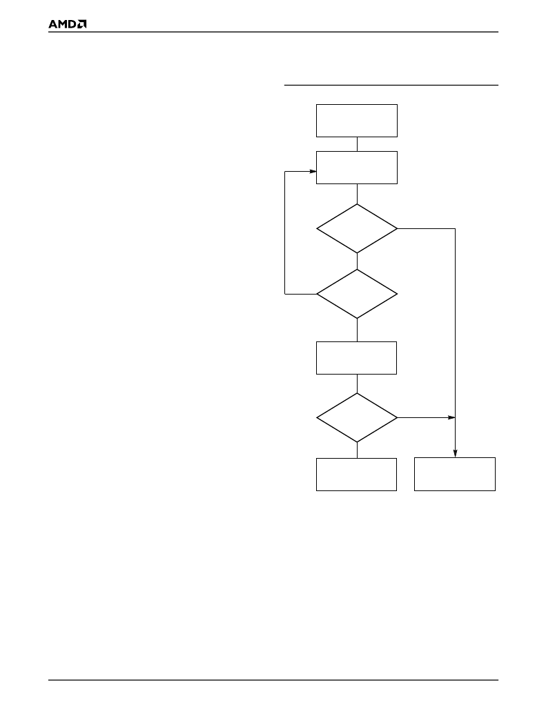
Figure 3 shows the Data# Polling algorithm.
DQ7 = Data
Yes
No
No
DQ5 = 1
No
Yes
Yes
FAIL
PASS
Read DQ7–DQ0
Addr = VA
Read DQ7–DQ0
Addr = VA
DQ7 = Data
START
Notes:
1. VA = Valid address for programming. During a sector
erase operation, a valid address is an address within any
sector selected for erasure. During chip erase, a valid
address is any non-protected sector address.
2.
DQ7 should be rechecked even if DQ5 = “1” because
DQ7 may change simultaneously with DQ5.
Figure 3.
Data# Polling Algorithm
相關(guān)PDF資料 |
PDF描述 |
|---|---|
| AM29LV400BB-120DTC1 | EEPROM |
| AM29LV400BB-120DTE1 | EEPROM |
| AM29LV400BB-120DTI1 | EEPROM |
| AM29LV400BB-120DWC1 | EEPROM |
| AM29LV400BB-120DWE1 | EEPROM |
相關(guān)代理商/技術(shù)參數(shù) |
參數(shù)描述 |
|---|---|
| AM29LV400BB-120EC | 制造商:Spansion 功能描述:Flash Mem Parallel 3V/3.3V 4M-Bit 512K x 8/256K x 16 120ns 48-Pin TSOP |
| AM29LV400BB-120EI | 制造商:Spansion 功能描述:NOR Flash Parallel 3V/3.3V 4Mbit 512K/256K x 8bit/16bit 120ns 48-Pin TSOP |
| AM29LV400BB-120SC | 制造商:Spansion 功能描述:NOR Flash Parallel 3V/3.3V 4Mbit 512K/256K x 8bit/16bit 120ns 44-Pin SOP |
| AM29LV400BB-120WAI | 制造商:Spansion 功能描述:Flash Mem Parallel 3V/3.3V 4M-Bit 512K x 8/256K x 16 120ns 48-Pin FBGA |
| AM29LV400BB-55RWAI | 制造商:Spansion 功能描述:SPZAM29LV400BB-55RWAI 4M FLASH EOL150606 |
發(fā)布緊急采購,3分鐘左右您將得到回復(fù)。