- 您現(xiàn)在的位置:買賣IC網(wǎng) > PDF目錄64112 > AM55-0015ATR 2400 MHz - 2500 MHz RF/MICROWAVE NARROW BAND MEDIUM POWER AMPLIFIER PDF資料下載
參數(shù)資料
| 型號(hào): | AM55-0015ATR |
| 元件分類: | 放大器 |
| 英文描述: | 2400 MHz - 2500 MHz RF/MICROWAVE NARROW BAND MEDIUM POWER AMPLIFIER |
| 封裝: | PLASTIC, QSOP-28 |
| 文件頁(yè)數(shù): | 1/8頁(yè) |
| 文件大小: | 177K |
| 代理商: | AM55-0015ATR |
n North America: Tel. (800) 366-2266, Fax (800) 618-8883
n Asia/Pacific: Tel.+81-44-844-8296, Fax +81-44-844-8298
n Europe: Tel. +44 (1344) 869 595, Fax+44 (1344) 300 020
Specifications subject to change without notice.
Visit www.macom.com for additional data sheets and product information.
V 2.0
Features
Highly Integrated Power Amplifier with T/R Switch
Operates with 2.7 V to 6 V Supply Voltage
High Linear Output Power (P
1dB: +24 dBm Typical)
Individual Gate Control for Each Amplifier Stage
Low Cost QSOP-28 Plastic Package
Description
M/A-COM’s AM55-0015 is a GaAs power amplifier with an
integrated transmit/receive switch in a low cost QSOP-28
plastic package. The power amplifier delivers +24 dBm of
linear power with high efficiency and can be operated with
voltages as low as 2.7 volts. The power amplifier switch is fully
monolithic. The T/R switch achieves good insertion loss and
isolation without degrading the overall linearity. The switch can
be controlled with CMOS logic levels.
The AM55-0015 is ideally suited for QPSK, BPSK or other
linearly modulated systems in the 2.4 GHz ISM frequency band.
It can also be used in GFSK systems where levels of +25 dBm
are required. Typical applications include WLAN and wireless
portable data collection.
M/A-COM's AM55-0015 is fabricated using a mature 0.5
micron gate length GaAs process. The process features full
passivation for increased performance and reliability.
Am55-0015
250 mW Power Amplifier with T/R Switch
2.4 - 2.5 GHz
1
1. If specific reel size is required, consult factory for part number
assignment
Ordering Information
Part Number
Package
AM55-0015
QSOP-28, 28-Lead Plastic Pkg.
AM55-0015TR
Forward Tape and Reel
1
AM55-0015RTR
Reverse Tape and Reel
1
AM55-0015SMB
Designer’s Kit
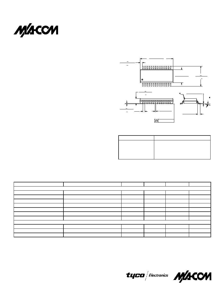
QSOP-28
.004 (0,10)
.3900
0-8
9,91 +0,09
-0,1
+.0037
-.0041
+.0025
+0,06
0,7
.0275
-.0043
+.0034
-0,11
+0,09
3,91
.1540
.236
5,99 +0,2
+.008
+.003
+0,08
1,45
.057
1,45+0,08
+.003
0,64
.025
.010
0,25+0,1
-0,03
+.004
-.001
-.0005
+.0018
-0,01
+0,05
0,2
.0080
.015 (0,38) X 45
.028
0,71
+0,56
-0,33
+.022
-.013
Dimensions are inches over millimeters.
1. Refer to External Circuitry Diagram for Gate Bias Current
Electrical Specifications: VDD1,2,3 = +5V ± 5%, VGG adjusted for total drain current of 180 mA
1, T
A = 25°C
Parameter
Test Conditions
Units
Min.
Typ.
Max.
POWER AMPLIFIER
Linear Gain
Frequency = 2.45 GHz
dB
27
29
32
VSWR In/Out
Frequency = 2.45 GHz
—
1.75:1
—
Output Power @ P1dB
Frequency = 2.45 GHz
dBm
22.5
24.5
—
Second Harmonic @ P1dB
Frequency = 2.45 GHz
dBm
—
-20
0
Third Harmonic @ P1dB
Frequency = 2.45 GHz
dBm
—
-30
-10
IDD @ P1dB (VDD1+VDD2+VDD3)
Frequency = 2.45 GHz
dB
—
270
375
Saturated Power
Frequency = 2.45 GHz, PIN = -3 dBm
dBm
24.5
25.5
—
T/R SWITCH
Insertion Loss
Frequency = 2.45 GHz
dB
—
1.2
1.5
Isolation
Frequency = 2.45 GHz
dB
10
12
—
VSWR In/Out
Frequency = 2.45 GHz
—
1.5:1
—
相關(guān)PDF資料 |
PDF描述 |
|---|---|
| AMC-132 | 5 MHz - 200 MHz RF/MICROWAVE WIDE BAND MEDIUM POWER AMPLIFIER |
| AM-132 | 5 MHz - 200 MHz RF/MICROWAVE WIDE BAND MEDIUM POWER AMPLIFIER |
| AMC-138 | 5 MHz - 200 MHz RF/MICROWAVE WIDE BAND MEDIUM POWER AMPLIFIER |
| AMC-140SMA | 10 MHz - 200 MHz RF/MICROWAVE WIDE BAND MEDIUM POWER AMPLIFIER |
| AMC-145SMA | 10 MHz - 1000 MHz RF/MICROWAVE WIDE BAND LOW POWER AMPLIFIER |
相關(guān)代理商/技術(shù)參數(shù) |
參數(shù)描述 |
|---|---|
| AM55-0016 | 制造商:MA-COM 制造商全稱:M/A-COM Technology Solutions, Inc. 功能描述:Switched Low Noise Amplifier 800 - 1000 MHz |
| AM55-0016_1 | 制造商:MA-COM 制造商全稱:M/A-COM Technology Solutions, Inc. 功能描述:Switched Low Noise Amplifier 800 - 1000 MHz |
| AM55-0016RTR | 制造商:MA-COM 制造商全稱:M/A-COM Technology Solutions, Inc. 功能描述:Switched Low Noise Amplifier 800 - 1000 MHz |
| AM55-0016SMB | 制造商:MA-COM 制造商全稱:M/A-COM Technology Solutions, Inc. 功能描述:Switched Low Noise Amplifier 800 - 1000 MHz |
| AM55-0016TR | 制造商:M/A-COM Technology Solutions 功能描述:RF AMP CHIP SGL GP 1GHZ 5V 8MSOP - Tape and Reel |
發(fā)布緊急采購(gòu),3分鐘左右您將得到回復(fù)。