- 您現(xiàn)在的位置:買賣IC網(wǎng) > PDF目錄362307 > AMD29DL163DB120EI EEPROM PDF資料下載
參數(shù)資料
| 型號(hào): | AMD29DL163DB120EI |
| 元件分類: | EEPROM |
| 英文描述: | EEPROM |
| 中文描述: | EEPROM的 |
| 文件頁數(shù): | 9/53頁 |
| 文件大小: | 1167K |
| 代理商: | AMD29DL163DB120EI |
第1頁第2頁第3頁第4頁第5頁第6頁第7頁第8頁當(dāng)前第9頁第10頁第11頁第12頁第13頁第14頁第15頁第16頁第17頁第18頁第19頁第20頁第21頁第22頁第23頁第24頁第25頁第26頁第27頁第28頁第29頁第30頁第31頁第32頁第33頁第34頁第35頁第36頁第37頁第38頁第39頁第40頁第41頁第42頁第43頁第44頁第45頁第46頁第47頁第48頁第49頁第50頁第51頁第52頁第53頁
July 29, 2002
Am29DL16xD
9
DEVICE BUS OPERATIONS
This section describes the requirements and use of
the device bus operations, which are initiated through
the internal command register. The command register
itself does not occupy any addressable memory loca-
tion. The register is a latch used to store the
commands, along with the address and data informa-
tion needed to execute the command. The contents of
the register serve as inputs to the internal state ma-
chine. The state machine outputs dictate the function
of the device. Table 1 lists the device bus operations,
the inputs and control levels they require, and the re-
sulting output. The following subsections describe
each of these operations in further detail.
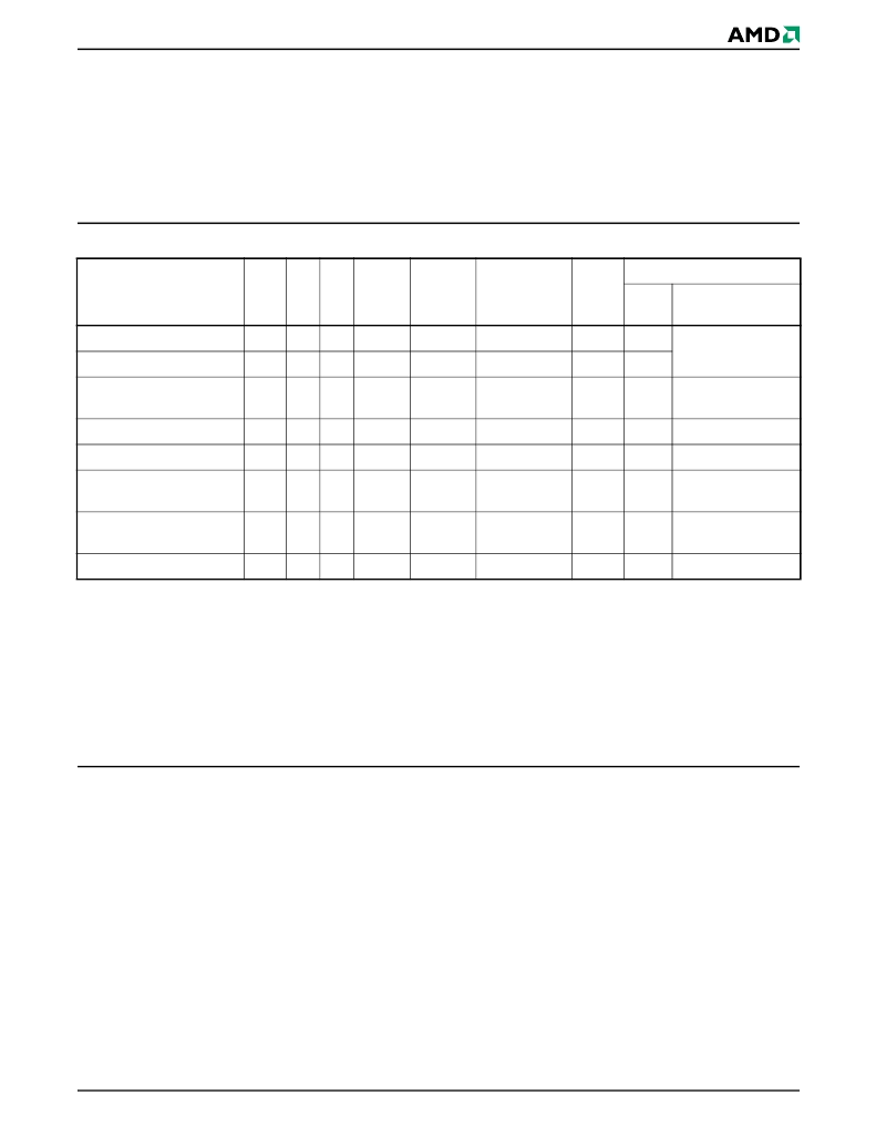
Table 1.
Am29DL16xD Device Bus Operations
Legend:
L = Logic Low = V
IL
, H = Logic High = V
IH
, V
ID
= 8.5–12.5
V, V
HH
= 9.0 ± 0.5 V, X = Don’t Care, SA = Sector Address,
A
IN
= Address In, D
IN
= Data In, D
OUT
= Data Out
Notes:
1. Addresses are A19:A0 in word mode (BYTE# = V
IH
), A19:A-1 in byte mode (BYTE# = V
IL
).
2. The sector protect and sector unprotect functions may also be implemented via programming equipment. See the “Sector/Sector
Block Protection and Unprotection” section.
3. If WP#/ACC = V
IL
, the two outermost boot sectors remain protected. If WP#/ACC = V
IH
, the two outermost boot sector
protection depends on whether they were last protected or unprotected using the method described in “Sector/Sector Block
Protection and Unprotection”. If WP#/ACC = V
HH,
all sectors will be unprotected.
Word/Byte Configuration
The BYTE# pin controls whether the device data I/O
pins operate in the byte or word configuration. If the
BYTE# pin is set at logic ‘1’, the device is in word con-
figuration, DQ0–DQ15 are active and controlled by
CE# and OE#.
If the BYTE# pin is set at logic ‘0’, the device is in byte
configuration, and only data I/O pins DQ0–DQ7 are
active and controlled by CE# and OE#. The data I/O
pins DQ8–DQ14 are tri-stated, and the DQ15 pin is
used as an input for the LSB (A-1) address function.
Requirements for Reading Array Data
To read array data from the outputs, the system must
drive the CE# and OE# pins to V
IL
. CE# is the power
control and selects the device. OE# is the output con-
trol and gates array data to the output pins. WE#
should remain at V
IH
. The BYTE# pin determines
whether the device outputs array data in words or
bytes.
The internal state machine is set for reading array data
upon device power-up, or after a hardware reset. This
ensures that no spurious alteration of the memory
content occurs during the power transition. No com-
mand is necessary in this mode to obtain array data.
Standard microprocessor read cycles that assert valid
addresses on the device address inputs produce valid
data on the device data outputs. Each bank remains
enabled for read access until the command register
contents are altered.
Operation
CE#
OE# WE# RESET# WP#/ACC
Addresses
(Note 2)
DQ0–
DQ7
DQ8–DQ15
BYTE#
= V
IH
BYTE#
= V
IL
Read
L
L
H
H
L/H
A
IN
D
OUT
D
OUT
DQ8–DQ14 = High-Z,
DQ15 = A-1
Write
L
H
L
H
(Note 3)
A
IN
D
IN
D
IN
Standby
V
CC
±
0.3 V
X
X
V
CC
±
0.3 V
H
X
High-Z
High-Z
High-Z
Output Disable
L
H
H
H
L/H
X
High-Z
High-Z
High-Z
Reset
X
X
X
L
L/H
X
High-Z
High-Z
High-Z
Sector Protect (Note 2)
L
H
L
V
ID
L/H
SA, A6 = L,
A1 = H, A0 = L
D
IN
X
X
Sector Unprotect (Note 2)
L
H
L
V
ID
(Note 3)
SA, A6 = H,
A1 = H, A0 = L
D
IN
X
X
Temporary Sector Unprotect
X
X
X
V
ID
(Note 3)
A
IN
D
IN
D
IN
High-Z
相關(guān)PDF資料 |
PDF描述 |
|---|---|
| AMD29DL163DB120PCI | EEPROM |
| AMD29DL163DB120WCI | EEPROM |
| AMD29DL163DB70EI | EEPROM |
| AMD29DL163DB70PCI | EEPROM |
| AMD29DL163DB70WCI | EEPROM |
相關(guān)代理商/技術(shù)參數(shù) |
參數(shù)描述 |
|---|---|
| AMD29DL163DB120PCI | 制造商:未知廠家 制造商全稱:未知廠家 功能描述:EEPROM |
| AMD29DL163DB120WCI | 制造商:未知廠家 制造商全稱:未知廠家 功能描述:EEPROM |
| AMD29DL163DB70EI | 制造商:未知廠家 制造商全稱:未知廠家 功能描述:EEPROM |
| AMD29DL163DB70PCI | 制造商:未知廠家 制造商全稱:未知廠家 功能描述:EEPROM |
| AMD29DL163DB70WCI | 制造商:未知廠家 制造商全稱:未知廠家 功能描述:EEPROM |
發(fā)布緊急采購,3分鐘左右您將得到回復(fù)。