- 您現(xiàn)在的位置:買賣IC網(wǎng) > PDF目錄382855 > AMS682CP (Advanced Monolithic Systems, Inc.) INVERTING VOLTAGE DOUBLER PDF資料下載
參數(shù)資料
| 型號(hào): | AMS682CP |
| 廠商: | Advanced Monolithic Systems, Inc. |
| 英文描述: | INVERTING VOLTAGE DOUBLER |
| 中文描述: | 反向電壓倍增 |
| 文件頁數(shù): | 3/7頁 |
| 文件大小: | 62K |
| 代理商: | AMS682CP |
Advanced Monolithic Systems, Inc.
6680B Sierra Lane, Dublin, CA 94568 Phone (925) 556-9090 Fax (925) 556-9140
AMS682
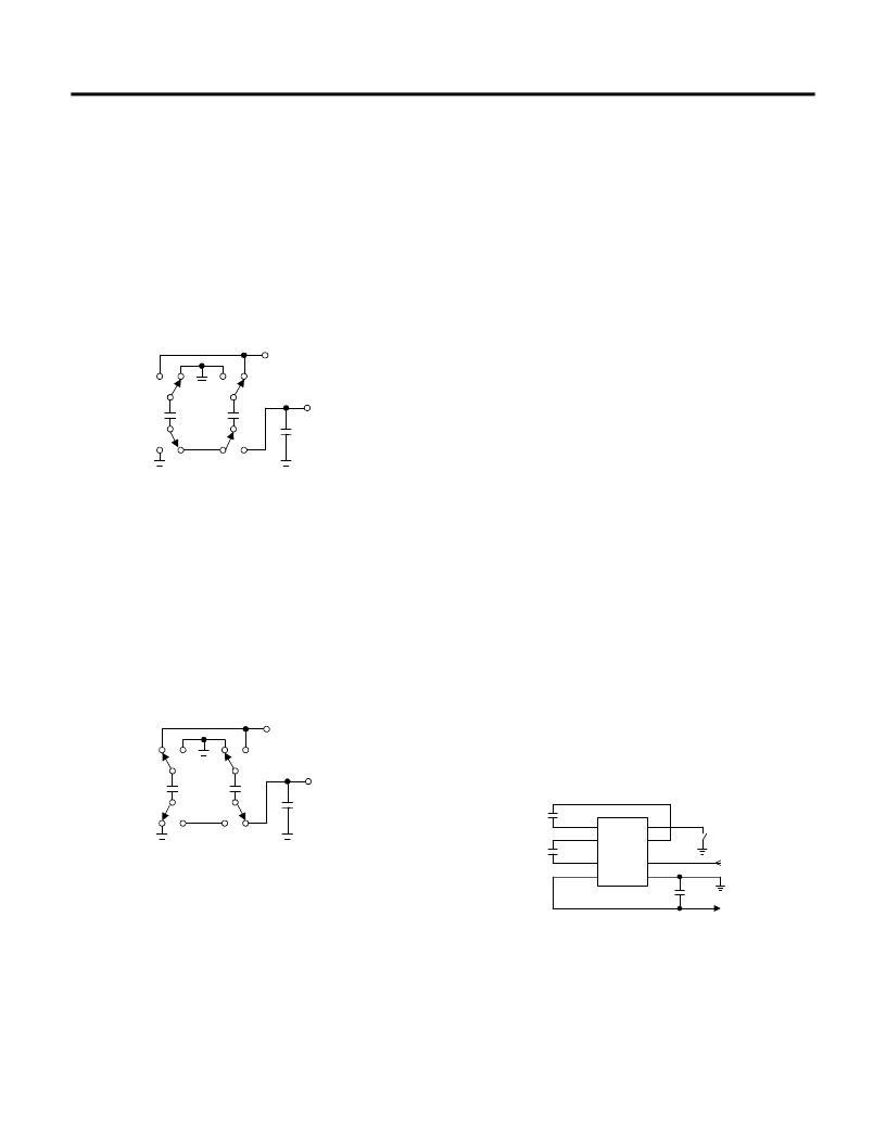
DETAILED DESCRIPTION
Phase 1
V
SS
charge storage- before this phase of the clock cycle,
capacitor C
1
is already charged to +5V. C
1+
is then switched
to ground and the charge in C
1-
is transferred to C
2-
.
Since C
2+
is at +5V, the voltage potential across capacitor C
2
is now -10V.
-
+
C
3
SW2
+
-
-5V
SW4
SW3
SW1
V
IN
=+5V
V
OUT
Figure 2. Charge Pump - Phase 1
Phase 2
V
SS
transfer- phase two of the clock connects the negative
terminal of C
2
to the negative side of reservoir capacitor C
3
and the positive terminal of C
2
to the ground, transferring the
generated -10V to C
3
. Simultaneously, the positive side of
capacitor C
1
is switched to +5V and the negative side is
connected to ground. C
2
is then switched to V
CC
and GND and
Phase 1 begins again.
-
+
C
3
SW2
SW4
+
-
-10V
SW3
SW1
V
IN
=+5V
V
OUT
Figure 3. Charge Pump - Phase 2
MAXIMUM OPERATING LIMITS
The AMS682 has on-chip zener diodes that clamp VIN to
approximately 5.8V, and V
-OUT
to -11.6V. Exceeding the
maximum supply voltage will potentially damage the chip.
With an input voltage of 2V to 5.5V the AMS682 will operate
over the entire operating temperature range.
EFFICIENCY CONSIDERATIONS
Theoretically a charge pump voltage multiplier can approach
100% efficiency under the following conditions:
The charge pump switches have virtually no offset and are
extremely low on resistance.
Minimal power is consumed by the drive circuitry.
The Impedances of the reservoir and pump capacitors are
negligible.
For the AMS682, efficiency is as shown below:
Voltage Efficiency = V
OUT
/ (-2V
IN
)
V
OUT
= -2V
IN
+ V
DROP
V
DROP
= (I
OUT
) (R
OUT
)
Power Loss = I
OUT
(V
DROP
)
There will be a substantial voltage difference between V
OUT
and
2V
IN
if the impedances of the pump capacitors C
1
and C
2
are
high with respect to their respective output loads.
If the values of the reservoir capacitor C
3
are larger the output
ripple will be reduced. The efficiency will be improved if both
pump and reservoir capacitors have larger values. ( See
“Capacitor Selection” in Application Section.)
APPLICATIONS
Negative Doubling Converter
The AMS682 is most commonly used as a charge pump voltage
converter which provides a negative output of two times a
positive input voltage (Fig.4)
GND
V
IN
6
4
V
-
OUT
5
7
2
3
1
C
1
C
2
-
+
C
1
+
C
2
V-
OUT
-
GND
V
IN
C
3
22
μ
F
+
+
+
22
μ
F
22
μ
F
C
1
C
2
ON/OFF8
Figure 4. Inverting Voltage Doubler
相關(guān)PDF資料 |
PDF描述 |
|---|---|
| AMS682CS | INVERTING VOLTAGE DOUBLER |
| AMS682EP | INVERTING VOLTAGE DOUBLER |
| AMS682ES | INVERTING VOLTAGE DOUBLER |
| AMS78L05L | 100mA VOLTAGE REGULATOR |
| AMS78LXX | 100mA VOLTAGE REGULATOR |
相關(guān)代理商/技術(shù)參數(shù) |
參數(shù)描述 |
|---|---|
| AMS682CS | 制造商:ADMOS 制造商全稱:ADMOS 功能描述:INVERTING VOLTAGE DOUBLER |
| AMS682EP | 制造商:ADMOS 制造商全稱:ADMOS 功能描述:INVERTING VOLTAGE DOUBLER |
| AMS682ES | 制造商:ADMOS 制造商全稱:ADMOS 功能描述:INVERTING VOLTAGE DOUBLER |
| AMS686/BIC | 制造商:Texas Instruments 功能描述: |
| AMS73CAG01168RALJH7 | 制造商:AMS 制造商全稱:AMS 功能描述:HIGH PERFORMANCE 1Gbit DDR3 SDRAM |
發(fā)布緊急采購,3分鐘左右您將得到回復(fù)。