- 您現(xiàn)在的位置:買賣IC網(wǎng) > PDF目錄376489 > AN6448NFBP (PANASONIC CORP) CAP 120PF 50V CERAMIC MONO 5% PDF資料下載
參數(shù)資料
| 型號: | AN6448NFBP |
| 廠商: | PANASONIC CORP |
| 元件分類: | 無繩電話/電話 |
| 英文描述: | CAP 120PF 50V CERAMIC MONO 5% |
| 中文描述: | TELEPHONE SPEECH CKT, PQFP64 |
| 封裝: | 14 X 14 MM, PLASTIC, QFP-64 |
| 文件頁數(shù): | 5/11頁 |
| 文件大小: | 156K |
| 代理商: | AN6448NFBP |
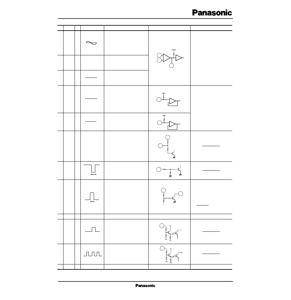
I
Pin Descriptions (cont.)
15OUT
16
O
MIC
IN
(+)
MIC
IN
(–)
I
I
17
18
MF–
IN
BT–
IN
DMC
DC–
CONT
I
I
I
O
I
I
I
19
20
21
22 CPC
NC
STR
CLK
NC
24
25
26
27
MIC preamp. input (1) :
A bias resistor and a microphone
connect to this pin.
MIC preamp. output :
R11 and C13 connected
between Pin17 and this pin
determine the f. characteristics.
The output impedance is 300
±
100
.
Feedback is input to this pin
through a capacitor. The
capacitor and R9 to R11, and
C12 and C13 determine the f.
characteristics.
The input impedance (10k
)
and C14 or C15 form an
input HPF.
Referring to the left figure, the
voltage, VCPC, at which
T
turns ON is calculated
as follows:
V
CPC
(ON)
=
R1
DTMF signal input :
DTMF signals are input through
a coupling capacitor C14.
When DMC is low at Pin20,
DTMF is enabled.
Input impedance is 10k
.
Dial mute control :
Normal speech mode when Pin20
is high or open (MIC amp. ON
and rec. amp. ON).
DTMF mode when Pin20 is low
(DTMF amp. ON and BT amp.
ON).
Line voltage control :
Line voltage is normal when this
pin is high. Line voltage increas-
es by 1 to 1.5V when this pin is
low.
Line interruption detector output :
This is an open collector output
to a microprocessor, requiring a
pull-up resistor connected to the
microprocessor's power supply.
This pin goes low when line
voltage is 3.0V or more, and
goes high when 1.5V or less.
No connection
Strobe signal input :
The strobe signal for serial control
data is input to this pin. The rising
edge of the strobe signal deter-
mines the timing at which internal
control address or ON/OFF status
is validated.
Clock signal input :
The clock signal for serial control
data is input to this pin. The rising
edge of the clock signal determines
the timing at which data is
read.
No connection
MIC preamp. input (2) :
R11 and C13 connected
between Pin15 and this pin
determine the f. characteristics.
BT signal input :
Beep tone (BT) signals are
input through a coupling
capacitor C15.
Input impedance is 10k
.
×
VBE (T
rCPC
)
= 2.5V (Ta=25C)
Description
Waveform
Remarks
PinNo.
Symbol
I/O
Equivalent Circuit
17
16
10k
+
–
V
REF
15
18
10k
V
REF
/SN
19
10k
V
REF
200k
100k
20
61
300k
V
CC
10k
26
200k
150k
21
144k
V
L
R2
R1
56k
22
2
Tr
CPC
300k
V
CC
10k
25
+
–
+
–
+
–
V
REF
V
REF
With signal ON
V
REF
With signal ON
V
REF
V
CC
0.2V
Line voltage increases
V
CC
0.2V
Line interruption
5V
0V
5V
0V
相關(guān)PDF資料 |
PDF描述 |
|---|---|
| AN644 | QuickChip Design Example 2 Low Power Silicon BJT LNA for 1.9GHz |
| AN6454SH | Pager Direct Conversion FSK Demodulator Mixer IC |
| AN6472NFBP | Cordless Telephone Speech Network IC Incorporating Cross-Point Switch |
| AN649 | HFTA-04.0: Optical/Electrical Conversion in SDH/SONET Fiber Optic Systems |
| AN6500 | BUILT-IN REFERENCE VOLTAGE OPERATIONAL AMPLIFIERS |
相關(guān)代理商/技術(shù)參數(shù) |
參數(shù)描述 |
|---|---|
| AN645 | 制造商:MICROCHIP 制造商全稱:Microchip Technology 功能描述:USING KEELOQ㈢ TO GENERATE HOPPING PASSWORDS |
| AN6454SH | 制造商:PANASONIC 制造商全稱:Panasonic Semiconductor 功能描述:Pager Direct Conversion FSK Demodulator Mixer IC |
| AN6472NFBP | 制造商:PANASONIC 制造商全稱:Panasonic Semiconductor 功能描述:Cordless Telephone Speech Network IC Incorporating Cross-Point Switch |
| AN6474NFBQ | 制造商:未知廠家 制造商全稱:未知廠家 功能描述:Telephone Speech Circuit |
| AN6477FBP | 制造商:未知廠家 制造商全稱:未知廠家 功能描述:Telephone Speech Circuit |
發(fā)布緊急采購,3分鐘左右您將得到回復(fù)。