- 您現(xiàn)在的位置:買賣IC網(wǎng) > PDF目錄362354 > AP1117Y15 1A Low Dropout Positive Adjustable or Fixed-Mode Regulator PDF資料下載
參數(shù)資料
| 型號(hào): | AP1117Y15 |
| 元件分類: | 基準(zhǔn)電壓源/電流源 |
| 英文描述: | 1A Low Dropout Positive Adjustable or Fixed-Mode Regulator |
| 中文描述: | 1A低壓差正可調(diào)或固定模式穩(wěn)壓器 |
| 文件頁(yè)數(shù): | 4/11頁(yè) |
| 文件大?。?/td> | 221K |
| 代理商: | AP1117Y15 |
1A Low Dropout Positive Adjustable or Fixed-Mode Regulator
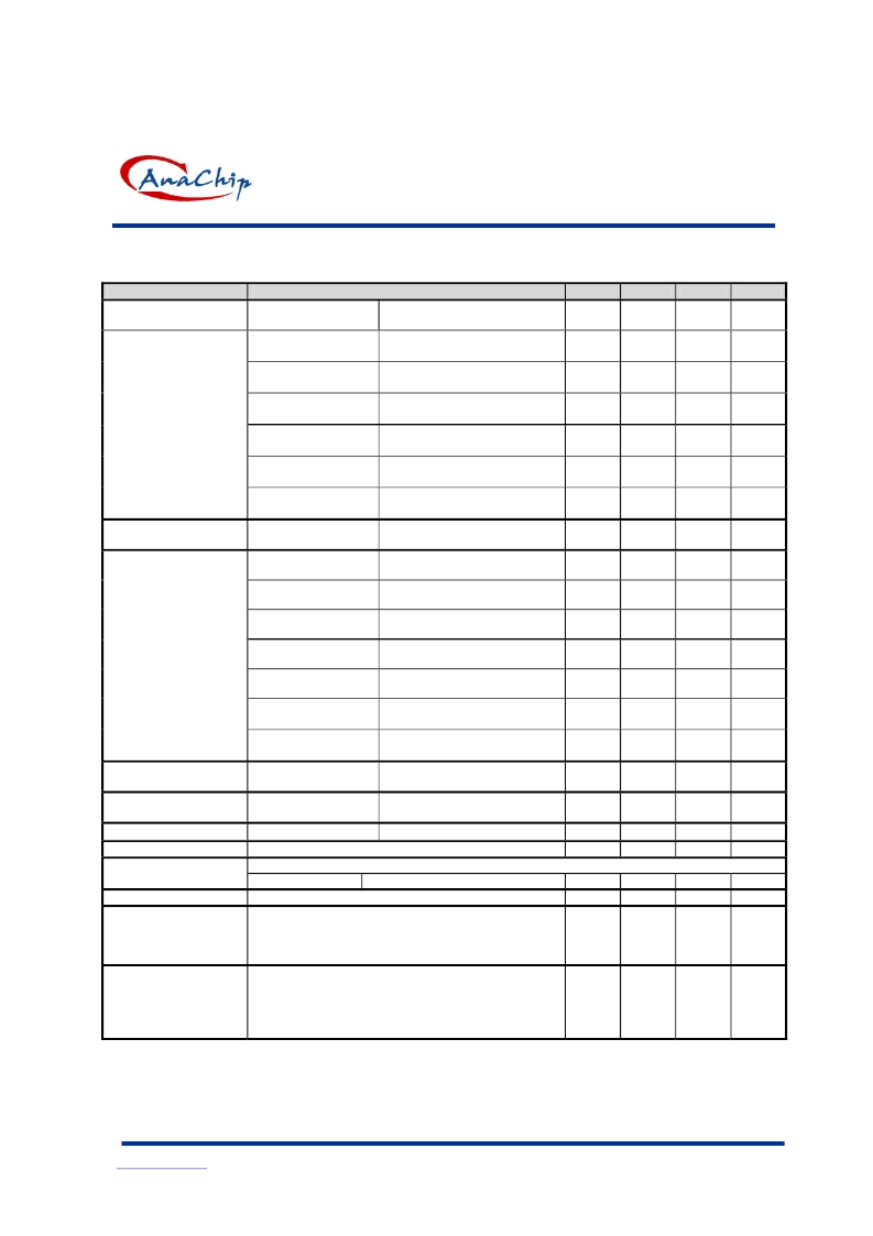
Electrical Characteristics
(Under Operating Conditions)
PARAMETER
AP1117
Anachip Corp.
www.anachip.com.tw
Rev.1.0 Aug 17, 2004
4/11
CONDITIONS
T
=25
o
C,(V
IN
-
OUT
)=1.5V
I
O
=10mA
I
= 10mA, T
J
= 25
o
C,
3V
≦
V
IN
≦
12V
I
OUT
= 10mA, T
J
= 25
o
C,
3.3V
≦
V
IN
≦
12V
I
= 10mA, T
= 25
o
C,
3.3V
≦
V
IN
≦
12V
I
OUT
= 10mA, T
J
= 25
o
C,
4V
≦
V
IN
≦
12V
I
OUT
= 10mA, T
J
= 25
o
C,
4.8V
≦
V
IN
≦
12V
I
OUT
= 10mA, T
J
= 25
o
C,
6.5V
≦
V
IN
≦
12V
I
O
=10mA,V
OUT
+1.5V<V
IN
<12V,
T
J
=25
C
V
IN
=3.3V,Vadj=0,0mA<Io<1A,
T
J
=25
C (Note 1,2)
V
IN
=3V, 0mA<Io<1A,
T
J
=25
C (Note 1,2)
V
IN
=3.3V, 0mA<Io<1A,
T
J
=25
C (Note 1,2)
V
IN
=3.3V, 0mA<Io<1A,
T
J
=25
C (Note 1,2)
V
IN
=4V, 0mA<Io<1A,
T
J
=25
C (Note 1,2)
V
IN
= 5V, 0
≦
I
OUT
≦
1A,
T
J
=25
o
C (Note 1,2)
V
IN
= 8V, 0
≦
I
OUT
≦
1A,
T
J
=25
o
C (Note 1,2)
MIN
TYP
MAX
UNIT
Reference Voltage
AP1117-ADJ
1.225
1.250
1.275
V
AP1117-1.5
1.470
1.500
1.530
V
AP1117-1.8
1.764
1.800
1.836
V
AP1117-1.9
1.862
1.900
1.938
V
AP1117-2.5
2.450
2.500
2.550
V
AP1117-3.3
3.235
3.300
3.365
V
Output Voltage
AP1117-5.0
4.900
5.000
5.100
V
Line Regulation
AP1117-XXX
0.2
%
AP1117-ADJ
1
%
AP1117-1.5
12
15
mV
AP1117-1.8
15
18
mV
AP1117-1.9
16
19
mV
AP1117-2.5
20
25
mV
AP1117-3.3
26
33
mV
Load Regulation
AP1117-5.0
40
50
mV
Dropout Voltage
(V
IN
-V
OUT
)
AP1117-ADJ/1.5/1.8
/1.9/2.5/3.3/5.0
AP1117-ADJ/1.5/1.8
/1.9/2.5/3.3/5.0
AP1117-XXX
T
A
=25
o
C, 30ms pulse
F=120Hz,C
OUT
=25uF Tantalum, I
OUT
=1A
AP1117-XXX
I
O
=10mA
SOT89
SOT-223
TO-252
TO-220/263
SOT89 : Control Circuitry/Power Transistor
SOT-223 : Control Circuitry/Power Transistor
TO-263
: Control Circuitry/Power Transistor
TO-252 : Control Circuitry/Power Transistor
TO-220 : Control Circuitry/Power Transistor
I
OUT
= 1A ,
V
OUT
=0.1%V
OUT
1.3
1.4
V
Current Limit
(V
IN
-V
OUT
) = 5V
1. 1
A
Minimum Load Current
Thermal Regulation
0
o
C
≦
Tj
≦
125
o
C
5
10
0.04
70
mA
%/W
dB
%
0.008
60
0.5
300
117
92
85
100
15
0.65/2.7
10
0.65/2.7
Ripple Rejection
V
IN
=V
OUT
+3V
Temperature Stability
θ
Thermal Resistance
Junction-to-Ambient(No
heat sink ;No air flow)
JA
O
C/W
JC
θ
Junction-to-Case
Thermal Resistance
O
C/W
Note1: See thermal regulation specifications for changes in output voltage due to heating effects. Line and load regulation are measured at a constant
junction temperature by low duty cycle pulse testing. Load regulation is measured at the output lead = 1/18” from the package.
Note2: Line and load regulation are guaranteed up to the maximum power dissipation of 15W. Power dissipation is determined by the difference between
input and output differential and the output current. Guaranteed maximum power dissipation will not be available over the full input/output range.
Note3: Quiescent current is defined as the minimum output current required in maintaining regulation. At 12V input/output differential the
device is guaranteed to regulate if the output current is greater than 10mA.
相關(guān)PDF資料 |
PDF描述 |
|---|---|
| AP1117Y15A | 1A Low Dropout Positive Adjustable or Fixed-Mode Regulator |
| AP1117Y15L | 1A Low Dropout Positive Adjustable or Fixed-Mode Regulator |
| AP1117Y15LA | 1A Low Dropout Positive Adjustable or Fixed-Mode Regulator |
| AP1117Y18 | 1A Low Dropout Positive Adjustable or Fixed-Mode Regulator |
| AP1117Y18A | 1A Low Dropout Positive Adjustable or Fixed-Mode Regulator |
相關(guān)代理商/技術(shù)參數(shù) |
參數(shù)描述 |
|---|---|
| AP1117Y-15 | 制造商:ANACHIP 制造商全稱:Anachip Corp 功能描述:1A Low Dropout Positive Adjustable or Fixed-Mode Regulator |
| AP1117Y15A | 制造商:ANACHIP 制造商全稱:Anachip Corp 功能描述:1A Low Dropout Positive Adjustable or Fixed-Mode Regulator |
| AP1117Y-15A | 制造商:ANACHIP 制造商全稱:Anachip Corp 功能描述:1A Low Dropout Positive Adjustable or Fixed-Mode Regulator |
| AP1117Y15G-13 | 功能描述:低壓差穩(wěn)壓器 - LDO LINEAR REG FIXED-MODE RoHS:否 制造商:Texas Instruments 最大輸入電壓:36 V 輸出電壓:1.4 V to 20.5 V 回動(dòng)電壓(最大值):307 mV 輸出電流:1 A 負(fù)載調(diào)節(jié):0.3 % 輸出端數(shù)量: 輸出類型:Fixed 最大工作溫度:+ 125 C 安裝風(fēng)格:SMD/SMT 封裝 / 箱體:VQFN-20 |
| AP1117Y15G-U | 制造商:DIODES 制造商全稱:Diodes Incorporated 功能描述:1A LOW DROPOUT POSITIVE ADJUSTABLE OR FIXED-MODE REGULATOR |
發(fā)布緊急采購(gòu),3分鐘左右您將得到回復(fù)。