- 您現(xiàn)在的位置:買賣IC網(wǎng) > PDF目錄4377 > APA600-FG484A (Microsemi SoC)IC FPGA PROASIC+ 600K 484-FBGA PDF資料下載
參數(shù)資料
| 型號: | APA600-FG484A |
| 廠商: | Microsemi SoC |
| 文件頁數(shù): | 35/178頁 |
| 文件大小: | 0K |
| 描述: | IC FPGA PROASIC+ 600K 484-FBGA |
| 標準包裝: | 40 |
| 系列: | ProASICPLUS |
| RAM 位總計: | 129024 |
| 輸入/輸出數(shù): | 370 |
| 門數(shù): | 600000 |
| 電源電壓: | 2.375 V ~ 2.625 V |
| 安裝類型: | 表面貼裝 |
| 工作溫度: | -40°C ~ 125°C |
| 封裝/外殼: | 484-BGA |
| 供應商設備封裝: | 484-FPBGA(23x23) |
第1頁第2頁第3頁第4頁第5頁第6頁第7頁第8頁第9頁第10頁第11頁第12頁第13頁第14頁第15頁第16頁第17頁第18頁第19頁第20頁第21頁第22頁第23頁第24頁第25頁第26頁第27頁第28頁第29頁第30頁第31頁第32頁第33頁第34頁當前第35頁第36頁第37頁第38頁第39頁第40頁第41頁第42頁第43頁第44頁第45頁第46頁第47頁第48頁第49頁第50頁第51頁第52頁第53頁第54頁第55頁第56頁第57頁第58頁第59頁第60頁第61頁第62頁第63頁第64頁第65頁第66頁第67頁第68頁第69頁第70頁第71頁第72頁第73頁第74頁第75頁第76頁第77頁第78頁第79頁第80頁第81頁第82頁第83頁第84頁第85頁第86頁第87頁第88頁第89頁第90頁第91頁第92頁第93頁第94頁第95頁第96頁第97頁第98頁第99頁第100頁第101頁第102頁第103頁第104頁第105頁第106頁第107頁第108頁第109頁第110頁第111頁第112頁第113頁第114頁第115頁第116頁第117頁第118頁第119頁第120頁第121頁第122頁第123頁第124頁第125頁第126頁第127頁第128頁第129頁第130頁第131頁第132頁第133頁第134頁第135頁第136頁第137頁第138頁第139頁第140頁第141頁第142頁第143頁第144頁第145頁第146頁第147頁第148頁第149頁第150頁第151頁第152頁第153頁第154頁第155頁第156頁第157頁第158頁第159頁第160頁第161頁第162頁第163頁第164頁第165頁第166頁第167頁第168頁第169頁第170頁第171頁第172頁第173頁第174頁第175頁第176頁第177頁第178頁
ProASICPLUS Flash Family FPGAs
v5.9
2-3
Clock Resources
The ProASICPLUS family offers powerful and flexible
control of circuit timing through the use of analog
circuitry. Each chip has two clock conditioning blocks
containing a phase-locked loop (PLL) core, delay lines,
phase shifter (0
° and 180°), clock multiplier/dividers, and
all
the
circuitry
needed
for
the
selection
and
interconnection of inputs to the global network (thus
providing bidirectional access to the PLL). This permits
the PLL block to drive inputs and/or outputs via the two
global lines on each side of the chip (four total lines).
This circuitry is discussed in more detail in the
Clock Trees
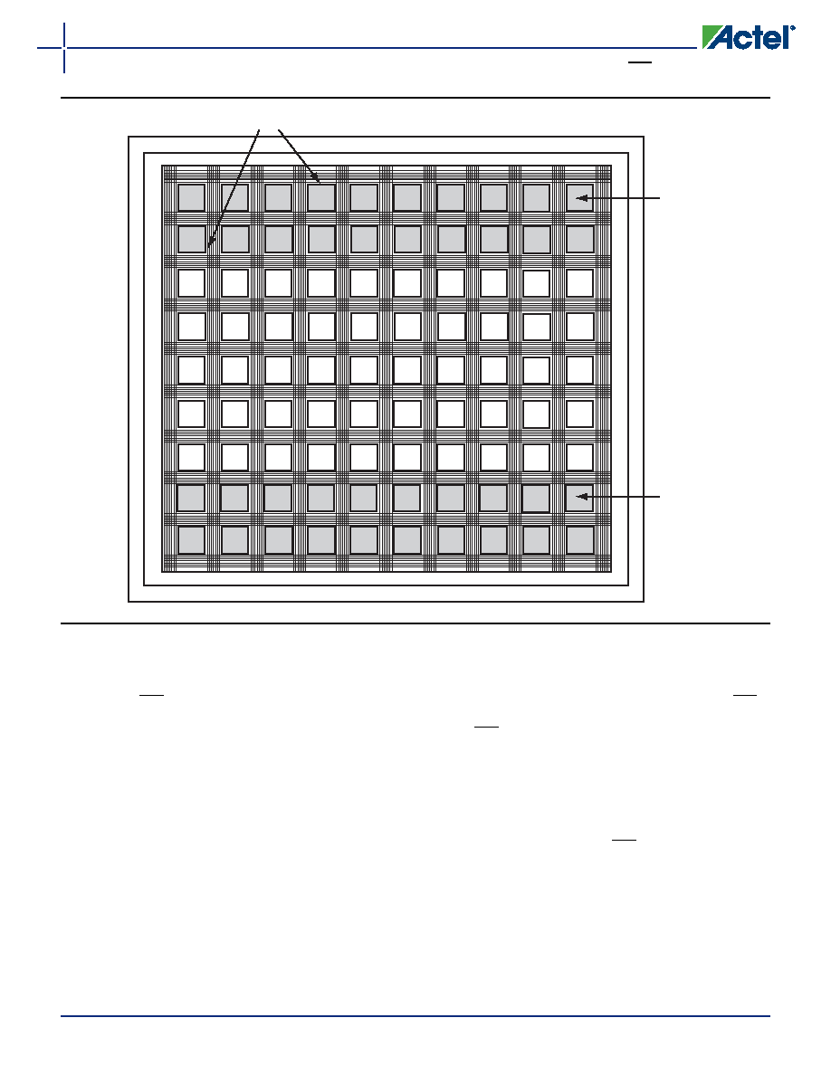
One of the main architectural benefits of ProASICPLUS is
the set of power- and delay-friendly global networks.
ProASICPLUS offers four global trees. Each of these trees
is based on a network of spines and ribs that reach all
the tiles in their regions (Figure 2-4 on page 2-4). This
flexible clock tree architecture allows users to map up to
88 different internal/external clocks in an APA1000
device. Details on the clock spines and various numbers
of the family are given in Table 2-1 on page 2-4.
The flexible use of the ProASICPLUS clock spine allows the
designer to cope with several design requirements. Users
implementing clock-resource intensive applications can
easily route external or gated internal clocks using global
routing spines. Users can also drastically reduce delay
penalties and save buffering resources by mapping
critical high fanout nets to spines. For design hints on
using these features, refer to Actel’s Efficient Use of
ProASIC Clock Trees application note.
Figure 2-3 High-Speed, Very Long-Line Resources
PAD RING
P
A
D
RING
I/O
RING
I/O
RING
High-Speed Very Long-Line Resouces
SRAM
相關PDF資料 |
PDF描述 |
|---|---|
| EP4CGX150CF23C7 | IC CYCLONE IV FPGA 150K 484FBGA |
| A42MX36-1BG272 | IC FPGA MX SGL CHIP 54K 272-PBGA |
| A42MX36-1BGG272 | IC FPGA MX SGL CHIP 54K 272-PBGA |
| EP4CGX110DF31C7 | IC CYCLONE IV FPGA 110K 896FBGA |
| A42MX36-1PQG208I | IC FPGA MX SGL CHIP 54K 208-PQFP |
相關代理商/技術參數(shù) |
參數(shù)描述 |
|---|---|
| APA600-FG484I | 功能描述:IC FPGA PROASIC+ 600K 484-FBGA RoHS:否 類別:集成電路 (IC) >> 嵌入式 - FPGA(現(xiàn)場可編程門陣列) 系列:ProASICPLUS 產(chǎn)品培訓模塊:Three Reasons to Use FPGA's in Industrial Designs Cyclone IV FPGA Family Overview 特色產(chǎn)品:Cyclone? IV FPGAs 標準包裝:60 系列:CYCLONE® IV GX LAB/CLB數(shù):9360 邏輯元件/單元數(shù):149760 RAM 位總計:6635520 輸入/輸出數(shù):270 門數(shù):- 電源電壓:1.16 V ~ 1.24 V 安裝類型:表面貼裝 工作溫度:0°C ~ 85°C 封裝/外殼:484-BGA 供應商設備封裝:484-FBGA(23x23) |
| APA600-FG676 | 功能描述:IC FPGA PROASIC+ 600K 676-FBGA RoHS:否 類別:集成電路 (IC) >> 嵌入式 - FPGA(現(xiàn)場可編程門陣列) 系列:ProASICPLUS 產(chǎn)品培訓模塊:Three Reasons to Use FPGA's in Industrial Designs Cyclone IV FPGA Family Overview 特色產(chǎn)品:Cyclone? IV FPGAs 標準包裝:60 系列:CYCLONE® IV GX LAB/CLB數(shù):9360 邏輯元件/單元數(shù):149760 RAM 位總計:6635520 輸入/輸出數(shù):270 門數(shù):- 電源電壓:1.16 V ~ 1.24 V 安裝類型:表面貼裝 工作溫度:0°C ~ 85°C 封裝/外殼:484-BGA 供應商設備封裝:484-FBGA(23x23) |
| APA600-FG676I | 功能描述:IC FPGA PROASIC+ 600K 676-FBGA RoHS:否 類別:集成電路 (IC) >> 嵌入式 - FPGA(現(xiàn)場可編程門陣列) 系列:ProASICPLUS 標準包裝:1 系列:ProASICPLUS LAB/CLB數(shù):- 邏輯元件/單元數(shù):- RAM 位總計:129024 輸入/輸出數(shù):248 門數(shù):600000 電源電壓:2.3 V ~ 2.7 V 安裝類型:表面貼裝 工作溫度:- 封裝/外殼:352-BFCQFP,帶拉桿 供應商設備封裝:352-CQFP(75x75) |
| APA600-FG896A | 制造商:ACTEL 制造商全稱:Actel Corporation 功能描述:Automotive-Grade ProASIC Flash Family FPGAs |
| APA600-FGB | 制造商:ACTEL 制造商全稱:Actel Corporation 功能描述:ProASIC Flash Family FPGAs |
發(fā)布緊急采購,3分鐘左右您將得到回復。