- 您現(xiàn)在的位置:買賣IC網(wǎng) > PDF目錄36703 > APT100GT60LR (MICROSEMI POWER PRODUCTS GROUP) 148 A, 600 V, N-CHANNEL IGBT, TO-264AA PDF資料下載
參數(shù)資料
| 型號: | APT100GT60LR |
| 廠商: | MICROSEMI POWER PRODUCTS GROUP |
| 元件分類: | IGBT 晶體管 |
| 英文描述: | 148 A, 600 V, N-CHANNEL IGBT, TO-264AA |
| 封裝: | TO-264, 3 PIN |
| 文件頁數(shù): | 2/6頁 |
| 文件大小: | 167K |
| 代理商: | APT100GT60LR |
052-6297
Rev
B
6
-
2010
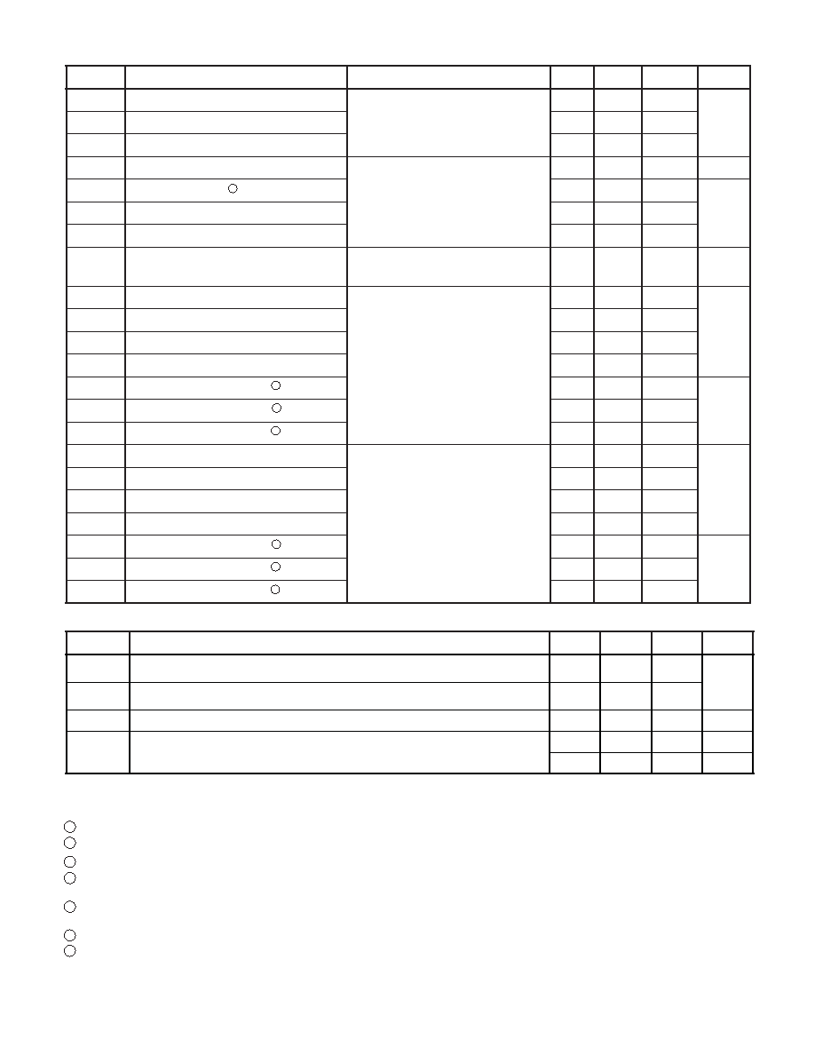
Dynamic Characteristic
APT100GT60B2R_LR(G)
Symbol
Characteristic
Test Conditions
Min
Typ
Max
Unit
C
ies
Input Capacitance
V
GE = 0V, VCE = 25V
f = 1MHz
-
5150
-
pF
C
oes
Output Capacitance
-
475
-
C
res
Reverse Transfer Capacitance
-
295
-
V
GEP
Gate-to-Emitter Plateau Voltage
Gate Charge
V
GE = 15V
V
CE= 300V
I
C = 100A
-
8.0
-
V
Q
g
Total Gate Charge 3
-
460
-
nC
Q
ge
Gate-Emitter Charge
-
40
-
Q
gc
Gate-Collector Charge
-
210
-
SSOA
Switching Safe Operating Area
T
J = 150°C, RG = 4.3Ω , VGE = 15V,
L = 100μH, V
CE= 600V
300
A
t
d(on)
Turn-On Delay Time
Inductive Switching (25°C)
V
CC = 400V
V
GE = 15V
I
C = 100A
R
G = 4.3Ω
T
J = +25°C
-40
-
ns
t
r
Current Rise Time
-
75
-
t
d(off)
Turn-Off Delay Time
-
320
-
t
f
Current Fall Time
-
100
-
E
on1
Turn-On Switching Energy 4
-
3250
-
μJ
E
on2
Turn-On Switching Energy 5
-
3525
-
E
off
Turn-Off Switching Energy 6
-
3125
-
t
d(on)
Turn-On Delay Time
Inductive Switching (125°C)
V
CC = 400V
V
GE = 15V
I
C = 100A
R
G = 4.3Ω
T
J = +125°C
-40
-
ns
t
r
Current Rise Time
-
75
-
t
d(off)
Turn-Off Delay Time
-
350
-
t
f
Current Fall Time
-
100
-
E
on1
Turn-On Switching Energy 4
-
3275
-
μJ
E
on2
Turn-On Switching Energy 5
-
4650
-
E
off
Turn-Off Switching Energy 6
-
3750
-
Symbol
Characteristic / Test Conditions
Min
Typ
Max
Unit
R
θJC
Junction to Case (IGBT)
-
0.25
°C/W
R
θJC
Junction to Case (DIODE)
-
N/A
W
T
Package Weight
-
29.2
-
g
Torque
Terminals and Mounting Screws
-
10
inlbf
-
1.1
Nm
1 Repetitive Rating: Pulse width limited by maximum junction temperature.
2 For Combi devices, I
ces includes both IGBT and FRED leakages.
3 See MIL-STD-750 Method 3471.
4 E
on1 is the clamped inductive turn-on energy of the IGBT only, without the effect of a commutating diode reverse recovery current adding to
z a the IGBT turn-on loss. Tested in inductive switching test circuit shown in gure 21, but with a Silicon Carbide diode.
5 E
on2 is the clamped inductive turn-on energy that includes a commutating diode reverse recovery current in the IGBT turn-on switching
loss. (See Figures 21, 22.)
6 E
off is the clamped inductive turn-off energy measured in accordance with JEDEC standard JESD24-1. (See Figures 21, 23.)
7 R
G is external gate resistance not including gate driver impedance.
Thermal and Mechanical Characteristics
Microsemi reserves the right to change, without notice, the specications and information contained herein.
相關(guān)PDF資料 |
PDF描述 |
|---|---|
| APT106N60B2C6 | 106 A, 600 V, 0.035 ohm, N-CHANNEL, Si, POWER, MOSFET |
| APT10M07JVR | 225 A, 100 V, 0.007 ohm, N-CHANNEL, Si, POWER, MOSFET |
| APT10M09B2VFRG | 100 A, 100 V, 0.009 ohm, N-CHANNEL, Si, POWER, MOSFET |
| APT10M09LVFR | 100 A, 100 V, 0.009 ohm, N-CHANNEL, Si, POWER, MOSFET, TO-264AA |
| APT10M09B2VFR | 100 A, 100 V, 0.009 ohm, N-CHANNEL, Si, POWER, MOSFET |
相關(guān)代理商/技術(shù)參數(shù) |
參數(shù)描述 |
|---|---|
| APT100GT60LRG | 制造商:MICROSEMI 制造商全稱:Microsemi Corporation 功能描述:Thunderbolt IGBT |
| APT100M50J | 功能描述:MOSFET N-CH 500V 100A SOT-227 RoHS:是 類別:半導體模塊 >> FET 系列:- 標準包裝:10 系列:* |
| APT100M50J_09 | 制造商:MICROSEMI 制造商全稱:Microsemi Corporation 功能描述:N-Channel MOSFET |
| APT100MC120JCU2 | 制造商:Microsemi Corporation 功能描述:SILICON CARBIDE DIODE |
| APT100S20B | 制造商:MICROSEMI 制造商全稱:Microsemi Corporation 功能描述:HIGH VOLTAGE SCHOTTKY DIODE |
發(fā)布緊急采購,3分鐘左右您將得到回復。