- 您現(xiàn)在的位置:買賣IC網(wǎng) > PDF目錄362442 > AS4C4M4F1-60JI x4 Fast Page Mode DRAM PDF資料下載
參數(shù)資料
| 型號(hào): | AS4C4M4F1-60JI |
| 英文描述: | x4 Fast Page Mode DRAM |
| 中文描述: | x4快速頁面模式的DRAM |
| 文件頁數(shù): | 6/19頁 |
| 文件大?。?/td> | 986K |
| 代理商: | AS4C4M4F1-60JI |
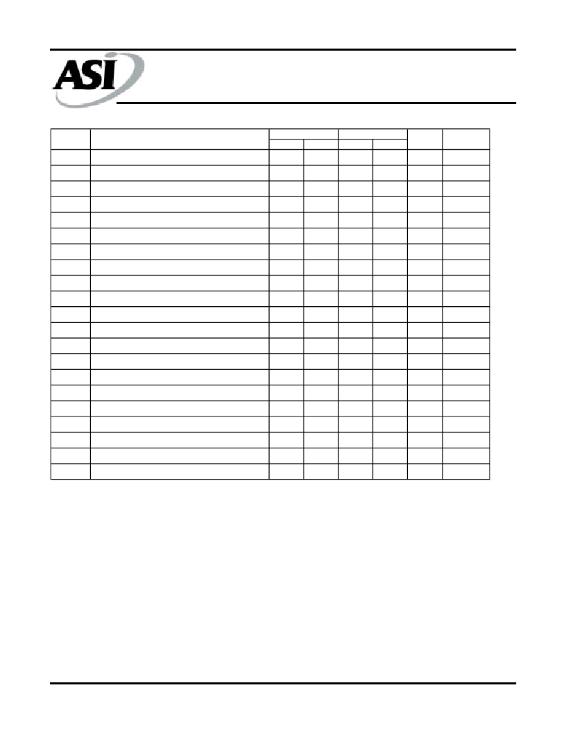
16 Me
g FPM DRAM
AS4C4M4
Austin Semiconductor, Inc.
Austin Semiconductor, Inc. reserves the right to change products or specifications without notice.
6
AS4C4M4
Rev. 1.0 5/03
TEST MODE CYCLE
11
MIN
115
MAX
MIN
135
MAX
t
RC
Random read or write cycle time
ns
t
RWC
Read-modify-write cycle time
160
180
ns
t
RAC
Access time from RAS\
65
70
ns
3, 4, 10, 12
t
CAC
Access time from CAS\
20
22
ns
3, 4, 5, 12
t
AA
Access time from column address
35
38
ns
3, 10 ,12
t
RAS
RAS\ pulse width
65
10K
75
10K
ns
t
CAS
CAS\ pulse width
20
10K
25
10K
ns
t
RSH
RAS\ hold time
20
22
ns
t
CSH
CAS\ hold time
65
70
ns
t
RAL
Column address to RAS\ lead time
35
40
ns
t
CWD
CAS\ to W\ delay time
45
48
ns
7
t
RWD
RAS\ to W\ delay time
90
100
ns
7
t
AWD
Column address to W\ delay time
60
70
ns
7
t
CPWD
CAS\ precharge to W\ delay time
65
70
ns
t
PC
Fast Page cycle time
45
50
ns
t
PRWC
Fast Page read-modify-write time
90
100
ns
t
RASP
RAS\ pulse width (Fast Page Cycle)
65
100K
75
100K
ns
t
CPA
Access time from CAS\ precharge
40
45
ns
3
t
OEA
OE\ access time
20
22
ns
t
OED
OE\ to data delay
20
22
ns
t
OEH
OE\ command hold time
20
22
ns
UNITS
NOTES
SYMBOL
PARAMETER
-60
-70
NOTES:
1. An initial pause of 200us is required after power-up followed by an 8 RAS\-only refresh or CAS\-before-RAS\ refresh cycles
before proper device operation is achieved.
2. V
(MIN) and V
(MAX) are reference levels for measuring timing of input signals. Transition times are measured between
V
(MIN) and V
(MAX) and are assumed to be 5ns for all inputs.
3. Measured with a load equivalent to 2 TTL loads and 100pF.
4. Operation within the t
(MAX) limit insures that t
(MAX) and be met. t
(MAX) is specified as a reference point only.
If t
is greater than the specified t
RCD
(MAX) limit, then access time is controlled exclusively by t
CAC
.
5. Assumes that t
RCD
> t
(MAX).
6. t
OFF
(MIN) and t
OEZ
(MAX) define the time at which the output achieves the open circuit condition and are not referenced V
OH
or V
OL
.
7. t
, t
, t
CWD
and t
AWD
are non restrictive operating parameters. They are included in the data sheet as electrical character-
istics only. If t
> t
duration of the cycle. If t
> t
(MIN), t
> t
(MIN) and t
> t
(MIN), then the cycle is a read-modify-write cycle
and the data output will contain the data read from the selected address. If neither of the above conditions is satisfied, the
condition of the data out is indeterminate.
(Continued on page 7)
相關(guān)PDF資料 |
PDF描述 |
|---|---|
| AS4C4M4F1-60TC | x4 Fast Page Mode DRAM |
| AS4C4M4F1-60TI | x4 Fast Page Mode DRAM |
| AS4C4M4F1Q-50JC | x4 Fast Page Mode DRAM |
| AS4LC4M4E0-60TI | x4 EDO Page Mode DRAM |
| AS4LC4M4E1 | 4M x 4 CMOS DRAM (EDO) Family |
相關(guān)代理商/技術(shù)參數(shù) |
參數(shù)描述 |
|---|---|
| AS4C4M4F1-60TC | 制造商:未知廠家 制造商全稱:未知廠家 功能描述:x4 Fast Page Mode DRAM |
| AS4C4M4F1-60TI | 制造商:未知廠家 制造商全稱:未知廠家 功能描述:x4 Fast Page Mode DRAM |
| AS4C4M4F1Q-50JC | 制造商:未知廠家 制造商全稱:未知廠家 功能描述:x4 Fast Page Mode DRAM |
| AS4C4M4F1Q-50TC | 制造商:未知廠家 制造商全稱:未知廠家 功能描述:DRAM|FAST PAGE|4MX4|CMOS|SOJ|28PIN|PLASTIC |
| AS4C4M4F1Q-60JC | 制造商:未知廠家 制造商全稱:未知廠家 功能描述:x4 Fast Page Mode DRAM |
發(fā)布緊急采購(gòu),3分鐘左右您將得到回復(fù)。