- 您現(xiàn)在的位置:買賣IC網(wǎng) > PDF目錄362444 > AS5SS128K36DQ-12IT x36 Fast Synchronous SRAM PDF資料下載
參數(shù)資料
| 型號(hào): | AS5SS128K36DQ-12IT |
| 英文描述: | x36 Fast Synchronous SRAM |
| 中文描述: | x36快速同步SRAM |
| 文件頁(yè)數(shù): | 10/16頁(yè) |
| 文件大?。?/td> | 224K |
| 代理商: | AS5SS128K36DQ-12IT |
第1頁(yè)第2頁(yè)第3頁(yè)第4頁(yè)第5頁(yè)第6頁(yè)第7頁(yè)第8頁(yè)第9頁(yè)當(dāng)前第10頁(yè)第11頁(yè)第12頁(yè)第13頁(yè)第14頁(yè)第15頁(yè)第16頁(yè)
SRAM
AS5SS128K36
Austin Semiconductor, Inc.
AS5SS128K36
Rev. 2.0 12/00
Austin Semiconductor, Inc. reserves the right to change products or specifications without notice.
10
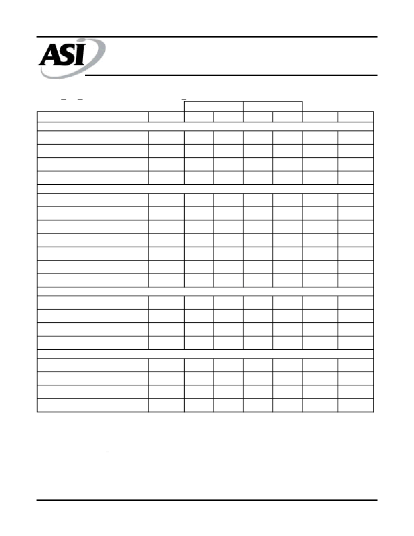
DESCRIPTION
SYM
MIN
MAX
MIN
MAX
UNITS
NOTES
CLOCK
Clock cycle time
t
KHKH
11
12
ns
Clock frequency
t
KF
90
83
MHz
Clock HIGH time
t
KHKL
3.0
3.0
ns
1
Clock LOW time
OUTPUT TIMES
Clock to output valid
t
KLKH
3.0
3.0
ns
1
t
KHQV
8.5
9.0
ns
Clock to output invalid
t
KHQX
3.0
3.0
ns
2
Clock to output in Low-Z
t
KHQX1
3.0
3.0
ns
2, 3, 4, 5
Clock to output in High-Z
t
KHQZ
5.0
5.0
ns
2, 3, 4, 5
OE\ to output valid
t
GLQV
5.0
5.0
ns
6
OE\ to output in Low-Z
t
GLQX
0
0
ns
2, 3, 4, 5
OE\ to output in High-Z
SETUP TIMES
Address
t
GHQZ
5.0
5.0
ns
2, 3, 4, 5
t
AVKH
2.2
2.5
ns
7
Clock enable (CKE\)
t
EVKH
2.2
2.5
ns
7
Control signals
t
CVKH
2.2
2.5
ns
7
Data-in
HOLD TIMES
Address
t
DVKH
2.2
2.5
ns
7
t
KHAX
0.5
0.5
ns
7
Clock enable (CKE\)
t
KHEX
0.5
0.5
ns
7
Control signals
t
KHCX
0.5
0.5
ns
7
Data-in
t
KHDX
0.5
0.5
ns
7
-11
-12
AC ELECTRICAL CHARACTERISTICS
6, 8, 9
(-55
o
C < T
A
< +125
o
C; V
DD,
V
DD
Q = +3.3V +0.165V)
NOTE:
1.
2.
3.
4.
5.
6.
7.
Measured as HIGH above V
and LOW below V
.
Contact ASI for more information on these parameters.
This parameter is sampled.
This parameter is measured with the output loading shown in Figure 2.
Transistion is measured +200mV from steady state voltage.
OE\ can be considerted a “Don’t Care” during WRITEs; however, controlling OE\ can help fine-tune a system for ZBL timing.
This is a synchrnous device. All addresses must meet the specified setup and hold times for all rising edgges o CLK when they are being
registered into the device. All other synchronous inputs must meet the setup and hold times with stable logic levels for all rising edges of
clock (CLK) when the chip is enabled. Chip enable must be valid at each rising edge of CLK when ADV/LD\ is LOW to remain enabled.
Test conditions as specified with the output loading shown in Figure 1, unless otherwise noted.
A WRITE cycle is defined by R/W\ LOW having been registered into the device at ADV/LD\ LOW. A READ cycle is defined by R/W\
HIGH with ADV/LD\ LOW. Both cases must meet setup and hold times.
8.
9.
相關(guān)PDF資料 |
PDF描述 |
|---|---|
| AS5SS128K36DQ-12XT | x36 Fast Synchronous SRAM |
| AS5SS128K36DQ-15 | x36 Fast Synchronous SRAM |
| AS5SS128K36DQ-9 | x36 Fast Synchronous SRAM |
| AS5SS256K18 | 256K x 18 SSRAM Synchronous Burst SRAM. Flow-Through |
| AS5SS256K18DB-10 | x18 Fast Synchronous SRAM |
相關(guān)代理商/技術(shù)參數(shù) |
參數(shù)描述 |
|---|---|
| AS5SS128K36DQ-12XT | 制造商:未知廠家 制造商全稱:未知廠家 功能描述:x36 Fast Synchronous SRAM |
| AS5SS128K36DQ-15 | 制造商:未知廠家 制造商全稱:未知廠家 功能描述:x36 Fast Synchronous SRAM |
| AS5SS128K36DQ-9 | 制造商:未知廠家 制造商全稱:未知廠家 功能描述:x36 Fast Synchronous SRAM |
| AS5SS256K18 | 制造商:未知廠家 制造商全稱:未知廠家 功能描述:256K x 18 SSRAM Synchronous Burst SRAM. Flow-Through |
| AS5SS256K18_05 | 制造商:AUSTIN 制造商全稱:Austin Semiconductor 功能描述:256K x 18 SSRAM Synchronous Burst SRAM, Flow-Through |
發(fā)布緊急采購(gòu),3分鐘左右您將得到回復(fù)。