- 您現(xiàn)在的位置:買賣IC網(wǎng) > PDF目錄362444 > AS6WA5128-HRI x8 SRAM PDF資料下載
參數(shù)資料
| 型號(hào): | AS6WA5128-HRI |
| 英文描述: | x8 SRAM |
| 中文描述: | x8的SRAM |
| 文件頁數(shù): | 6/9頁 |
| 文件大小: | 152K |
| 代理商: | AS6WA5128-HRI |
6
ALLIANCE SEMICONDUCTOR
10/6/00
AS6WA5128
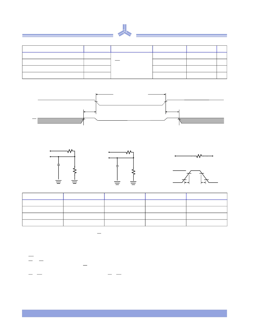
Data retention characteristics (over the operating range)
13,5
Parameter
V
CC
for data retention
Data retention current
Data retention waveform
AC test loads and waveforms
Notes
1
2
3
4
5
6
7
8
9
10 CS or WE must be HIGH during address transitions. Either CS or WE asserting high terminates a write cycle.
11 All write cycle timings are referenced from the last valid address to the first transitioning address.
12 N/A.
13 1.2V data retention applies to commercial and industrial temperature range operations.
14 C = 30pF, except at high Z and low Z parameters, where C = 5pF.
During V
CC
power-up, a pull-up resistor to V
CC
on CS is required to meet I
SB
specification.
This parameter is sampled, but not 100% tested.
For test conditions, see
AC Test Conditions
.
t
CLZ
and t
CHZ
are specified with C
L
= 5pF as in Figure C. Transition is measured ±500 mV from steady-state voltage.
This parameter is guaranteed, but not tested.
WE is HIGH for read cycle.
CS and OE are LOW for read cycle.
Address valid prior to or coincident with CS transition LOW.
All read cycle timings are referenced from the last valid address to the first transitioning address.
Symbol
V
DR
I
CCDR
t
CDR
t
R
Test conditions
Min
1.2V
Max
3.6
Unit
V
V
CC
= 1.2V
CS
≥
V
CC
– 0.1V or
V
IN
≥
V
CC
– 0.1V or
V
IN
≤
0.1V
–
4
mA
Chip deselect to data retention time
Operation recovery time
0
–
–
t
RC
ns
Parameters
V
CC
= 3.0V
1105
V
CC
= 2.5V
16670
V
CC
= 2.0V
15294
Unit
R1
Ohms
R2
R
TH
V
TH
1550
645
15380
8000
11300
6500
Ohms
Ohms
1.75V
1.2V
0.85V
Volts
V
CC
CS
t
R
t
CDR
Data retention mode
V
CC
V
CC
V
DR
≥
1.2V
V
IH
V
IH
V
DR
V
CC
R1
R2
OUTPUT
30 pF
INCLUDING
JIG AND
SCOPE
(a)
V
CC
R1
R2
OUTPUT
5 pF
ALL INPUT PULSES
(b)
10%
90%
10%
90%
GND
V
CC
Typ
< 5 ns
(c)
Thevenin equivalent:
OUTPUT
R
TH
V
INCLUDING
JIG AND
SCOPE
相關(guān)PDF資料 |
PDF描述 |
|---|---|
| AS6WA5128-STC | x8 SRAM |
| AS6WA5128-STI | x8 SRAM |
| AS6WA5128-TC | x8 SRAM |
| AS6WA5128-TI | x8 SRAM |
| AS6WA5128 | 3.0V to 3.6V 512K × 8 Intelliwatt low-power CMOS SRAM(3.0V 到 3.6V 512K × 8 Intelliwatt 低功耗 CMOS 靜態(tài)RAM) |
相關(guān)代理商/技術(shù)參數(shù) |
參數(shù)描述 |
|---|---|
| AS6WA5128-STC | 制造商:未知廠家 制造商全稱:未知廠家 功能描述:x8 SRAM |
| AS6WA5128-STI | 制造商:未知廠家 制造商全稱:未知廠家 功能描述:x8 SRAM |
| AS6WA5128-TC | 制造商:未知廠家 制造商全稱:未知廠家 功能描述:x8 SRAM |
| AS6WA5128-TI | 制造商:未知廠家 制造商全稱:未知廠家 功能描述:x8 SRAM |
| AS-6W-K | 制造商:FUJITSU 制造商全稱:Fujitsu Component Limited. 功能描述:MINIATURE RELAY 2 POLES-1 to 2 A (FOR SIGNAL SWITCHING) |
發(fā)布緊急采購,3分鐘左右您將得到回復(fù)。