- 您現(xiàn)在的位置:買賣IC網(wǎng) > PDF目錄379689 > ASC7521A (Electronic Theatre Controls, Inc.) LOW- OLTAGE 1-WIRE DIGITAL TEMPERATURE SENSOR PDF資料下載
參數(shù)資料
| 型號(hào): | ASC7521A |
| 廠商: | Electronic Theatre Controls, Inc. |
| 元件分類: | 溫度/濕度傳感器 |
| 英文描述: | LOW- OLTAGE 1-WIRE DIGITAL TEMPERATURE SENSOR |
| 中文描述: | 低OLTAGE 1 - Wire數(shù)字溫度傳感器 |
| 文件頁(yè)數(shù): | 14/18頁(yè) |
| 文件大?。?/td> | 186K |
| 代理商: | ASC7521A |
第1頁(yè)第2頁(yè)第3頁(yè)第4頁(yè)第5頁(yè)第6頁(yè)第7頁(yè)第8頁(yè)第9頁(yè)第10頁(yè)第11頁(yè)第12頁(yè)第13頁(yè)當(dāng)前第14頁(yè)第15頁(yè)第16頁(yè)第17頁(yè)第18頁(yè)
- 14 -
Andigilog, Inc. 2006
www.andigilog.com
October 2006 - 70A05011
aSC7521A
While it is important to minimize the distance to the remote
diode to reduce high-frequency noise pickup, they may be
located many feet away with proper shielding. Shielded,
twisted-pair cable is recommended, with the shield
connected only at the aSC7521A end as close as possible to
the ground pin of the device.
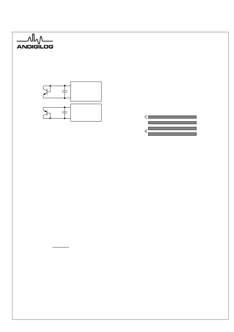
Figure 17 Discrete Remote Diode Connection
As with the CPU substrate diode, the temperature reported
will be subject to the same errors due to non-ideality variation
and series resistance. However, the transistor’s die
temperature is usually not the temperature of interest and
care must be taken to minimize the thermal resistance and
physical distance between that temperature and the remote
diode. The offset and response time will need to be
characterized by the user.
Series Resistance
Any external series resistance in the connections from the
aSC7521A to the CPU pins should be accounted for in
interpreting the results of a measurement.
The impact of series resistance on the measured
temperature is a result of measurement currents developing
offset voltages that add to the diode voltage. This is relatively
constant with temperature and may be corrected with a fixed
value in the offset register. To determine the temperature
impact of resistance is as follows:
Ω
°
×
=
°
×
=
Δ
Δ
×
×
=
Δ
or
/
675
.
/
200
135
μ
,
C
R
C
V
A
R
T
I
T
R
T
S
S
R
D
V
S
R
μ
where:
Δ
T
R
= difference in the temperature reading from actual.
R
= total series resistance of interconnect (both leads).
Δ
I
D
= difference in the two diode current levels (135μA).
T
= scale of temperature vs. V
BE
(200μV/°C).
S
V
For example, a total series resistance of 10
would give an
offset of +6.75°C.
Board Layout Considerations
The distance between the remote sensor and the aSC7521A
should be minimized. All wiring should be defended from high
frequency noise sources and a balanced differential layout
maintained on D+ and D-.
Any noise, both common-mode and differential, induced in
the remote diode interconnect may result in an offset in the
temperature reported. Circuit board layout should follow the
recommendation of Figure 18. Basically, use 10-mil lines and
spaces with grounds on each side of the differential pair.
Choose the ground plane closest to the CPU when using the
CPU’s remote diode.
Figure 18 Recommended Remote Diode Circuit
Board Interconnect
Noise filtering is accomplished by using a bypass capacitor
placed as close as possible to the aSC7521A D+ and D-
pins. A 1.0nF ceramic capacitor is recommended, but up to
3.3nF may be used. Additional filtering takes place within the
aSC7521A.
It is recommended that the following guidelines be used to
minimize noise and achieve highest accuracy:
1. Place a 0.1μF bypass capacitor to digital ground as
close as possible to the power pin of the aSC7521A.
2. Match the trace routing of the D+ and D- leads and
use a 1.0nF filter capacitor close to the aSC7521A.
Use ground runs along side the pair to minimize
differential coupling as in Figure 18.
3. Place the aSC7521A as close to the CPU or GPU
remote diode leads as possible to minimize noise and
series resistance.
4. Avoid running diode connections close to or in parallel
with high-speed busses, staying at least 2cm away.
5. Avoid running diode connections close to on-board
switching power supply inductors.
6. PC board leakage should be minimized by maintaining
minimum trace spacing and covering traces over their
full length with solder mask.
Thermal Considerations
The temperature of the aSC7521A will be close to that of the
PC board on which it is mounted. Conduction through the
leads is the primary path for heat flow. The reported local
10 mils
D +
D -
GND
10 mils
GND
D -
2N3904
D +
aSC7521A
2N3906
D +
aSC7521A
D -
相關(guān)PDF資料 |
PDF描述 |
|---|---|
| ASC7521AM8 | LOW- OLTAGE 1-WIRE DIGITAL TEMPERATURE SENSOR |
| ASC7531A | LOW-VOLTAGE 1-WIRE DIGITAL TEMPERATURE SENSOR AND VOLTAGE MONITOR |
| ASC7531AM10 | LOW-VOLTAGE 1-WIRE DIGITAL TEMPERATURE SENSOR AND VOLTAGE MONITOR |
| ASC7531B | LOW-VOLTAGE 1-WIRE DIGITAL TEMPERATURE SENSOR AND VOLTAGE MONITOR |
| ASC7531BM10 | LOW-VOLTAGE 1-WIRE DIGITAL TEMPERATURE SENSOR AND VOLTAGE MONITOR |
相關(guān)代理商/技術(shù)參數(shù) |
參數(shù)描述 |
|---|---|
| ASC7521AM8 | 制造商:未知廠家 制造商全稱:未知廠家 功能描述:LOW- OLTAGE 1-WIRE DIGITAL TEMPERATURE SENSOR |
| ASC7531A | 制造商:未知廠家 制造商全稱:未知廠家 功能描述:LOW-VOLTAGE 1-WIRE DIGITAL TEMPERATURE SENSOR AND VOLTAGE MONITOR |
| ASC7531AM10 | 制造商:未知廠家 制造商全稱:未知廠家 功能描述:LOW-VOLTAGE 1-WIRE DIGITAL TEMPERATURE SENSOR AND VOLTAGE MONITOR |
| ASC7531B | 制造商:未知廠家 制造商全稱:未知廠家 功能描述:LOW-VOLTAGE 1-WIRE DIGITAL TEMPERATURE SENSOR AND VOLTAGE MONITOR |
| ASC7531BM10 | 制造商:未知廠家 制造商全稱:未知廠家 功能描述:LOW-VOLTAGE 1-WIRE DIGITAL TEMPERATURE SENSOR AND VOLTAGE MONITOR |
發(fā)布緊急采購(gòu),3分鐘左右您將得到回復(fù)。