- 您現(xiàn)在的位置:買賣IC網(wǎng) > PDF目錄295111 > AT25080N-10SI (ATMEL CORP) SPI Serial EEPROMs PDF資料下載
參數(shù)資料
| 型號: | AT25080N-10SI |
| 廠商: | ATMEL CORP |
| 元件分類: | PROM |
| 英文描述: | SPI Serial EEPROMs |
| 中文描述: | 1K X 8 SPI BUS SERIAL EEPROM, PDSO8 |
| 封裝: | 0.150 INCH, PLASTIC, SOIC-8 |
| 文件頁數(shù): | 1/19頁 |
| 文件大?。?/td> | 279K |
| 代理商: | AT25080N-10SI |

1
Features
Serial Peripheral Interface (SPI) Compatible
Supports SPI Modes 0 (0,0) and 3 (1,1)
Low-voltage and Standard-voltage Operation
– 5.0 (V
CC = 4.5V to 5.5V)
– 2.7 (VCC = 2.7V to 5.5V)
– 1.8 (V
CC = 1.8V to 3.6V)
3.0 MHz Clock Rate (5V)
32-byte Page Mode
Block Write Protection
– Protect 1/4, 1/2, or Entire Array
Write Protect (WP) Pin and Write Disable Instructions for
both Hardware and Software Data Protection
Self-timed Write Cycle (5 ms Typical)
High-reliability
– Endurance: One Million Write Cycles
– Data Retention: 100 Years
Automotive Grade and Extended Temperature Devices Available
8-pin PDIP, 8-lead JEDEC SOIC, and 14-lead and 20-lead TSSOP Packages
Description
The AT25080/160/320/640 provides 8192/16384/32768/65536 bits of serial electri-
cally-erasable programmable read only memory (EEPROM) organized as
1024/2048/4096/8192 words of 8 bits each. The device is optimized for use in many
industrial and commercial applications where low-power and low-voltage operation
are essential. The AT25080/160/320/640 is available in space saving 8-pin PDIP, 8-
lead JEDEC SOIC, and 14-lead and 20-lead TSSOP packages.
SPI Serial
EEPROMs
8K (1024 x 8)
16K (2048 x 8)
32K (4096 x 8)
64K (8192 x 8)
AT25080
AT25160
AT25320
AT25640
Rev. 0675F–08/01
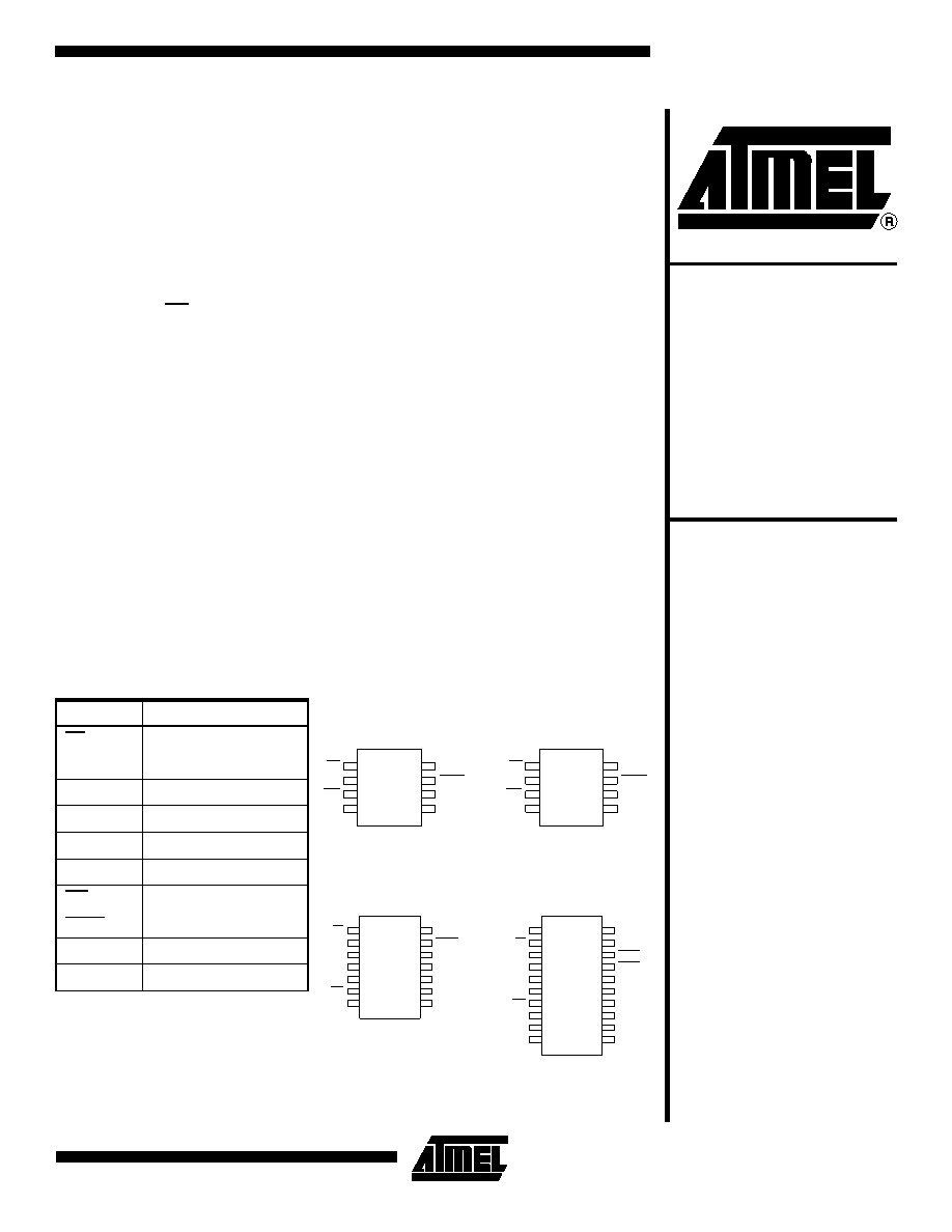
Pin Configuration
Pin Name
Function
CS
Chip Select
SCK
Serial Data Clock
SI
Serial Data Input
SO
Serial Data Output
GND
Ground
VCC
Power Supply
WP
Write Protect
HOLD
Suspends Serial Input
NC
No Connect
DC
Don’t Connect
8-pin PDIP
1
2
3
4
8
7
6
5
CS
SO
WP
GND
VCC
HOLD
SCK
SI
8-lead SOIC
1
2
3
4
8
7
6
5
CS
SO
WP
GND
VCC
HOLD
SCK
SI
14-lead TSSOP
1
2
3
4
5
6
7
14
13
12
11
10
9
8
CS
SO
NC
WP
GND
VCC
HOLD
NC
SCK
SI
20-lead TSSOP*
1
2
3
4
5
6
7
8
9
10
20
19
18
17
16
15
14
13
12
11
NC
CS
SO
NC
WP
GND
DC
NC
VCC
HOLD
NC
SCK
SI
DC
NC
Note:
*Pins 3, 4 and 17, 18 are internally connected
for 14-lead TSSOP socket compatibility.
(continued)
相關(guān)PDF資料 |
PDF描述 |
|---|---|
| AT25080-10PI-2.7 | SPI Serial EEPROMs |
| AT25080N-10SI-1.8 | SPI Serial EEPROMs |
| AT25080N-10SI-2.7 | SPI Serial EEPROMs |
| AT25080A-10PI-2.7 | SPI Serial EEPROMs |
| AT25080A-10TI-1.8 | SPI Serial EEPROMs |
相關(guān)代理商/技術(shù)參數(shù) |
參數(shù)描述 |
|---|---|
| AT25080N-10SI-1.8 | 制造商:ATMEL 制造商全稱:ATMEL Corporation 功能描述:SPI Serial EEPROMs |
| AT25080N-10SI-2.7 | 制造商:Atmel Corporation 功能描述:Serial EEPROM, 1K x 8, 8 Pin, Plastic, SOP |
| AT25080T1-10TC | 制造商:ATMEL 制造商全稱:ATMEL Corporation 功能描述:SPI Serial EEPROMs |
| AT25080T1-10TC-1.8 | 制造商:ATMEL 制造商全稱:ATMEL Corporation 功能描述:SPI Serial EEPROMs |
| AT25080T1-10TC-2.7 | 制造商:ATMEL 制造商全稱:ATMEL Corporation 功能描述:SPI Serial EEPROMs |
發(fā)布緊急采購,3分鐘左右您將得到回復(fù)。