- 您現(xiàn)在的位置:買賣IC網(wǎng) > PDF目錄1903 > AT89C51-24PI (Atmel)IC MICRO CTRL 24MHZ 40DIP PDF資料下載
參數(shù)資料
| 型號: | AT89C51-24PI |
| 廠商: | Atmel |
| 文件頁數(shù): | 14/17頁 |
| 文件大?。?/td> | 0K |
| 描述: | IC MICRO CTRL 24MHZ 40DIP |
| 標準包裝: | 9 |
| 系列: | 89C |
| 核心處理器: | 8051 |
| 芯體尺寸: | 8-位 |
| 速度: | 24MHz |
| 連通性: | UART/USART |
| 輸入/輸出數(shù): | 32 |
| 程序存儲器容量: | 4KB(4K x 8) |
| 程序存儲器類型: | 閃存 |
| RAM 容量: | 128 x 8 |
| 電壓 - 電源 (Vcc/Vdd): | 4 V ~ 6 V |
| 振蕩器型: | 內(nèi)部 |
| 工作溫度: | -40°C ~ 85°C |
| 封裝/外殼: | 40-DIP(0.600",15.24mm) |
| 包裝: | 管件 |
AT89C51
6
Programming the Flash
The AT89C51 is normally shipped with the on-chip Flash
memory array in the erased state (that is, contents = FFH)
and ready to be programmed. The programming interface
accepts either a high-voltage (12-volt) or a low-voltage
(V
CC) program enable signal. The low-voltage program-
ming mode provides a convenient way to program the
AT89C51 inside the user’s system, while the high-voltage
programming mode is compatible with conventional third-
party Flash or EPROM programmers.
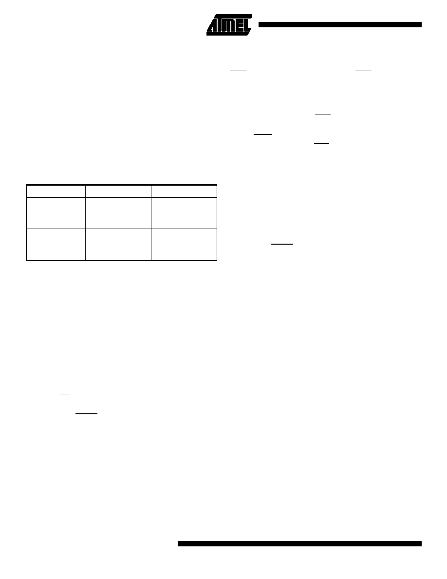
The AT89C51 is shipped with either the high-voltage or
low-voltage programming mode enabled. The respective
top-side marking and device signature codes are listed in
the following table.
The AT89C51 code memory array is programmed byte-by-
byte in either programming mode. To program any non-
blank byte in the on-chip Flash Memory, the entire memory
must be erased using the Chip Erase Mode.
Programming Algorithm: Before programming the
AT89C51, the address, data and control signals should be
set up according to the Flash programming mode table and
Figure 3 and Figure 4. To program the AT89C51, take the
following steps.
1.
Input the desired memory location on the address
lines.
2.
Input the appropriate data byte on the data lines.
3.
Activate the correct combination of control signals.
4.
Raise EA/V
PP to 12V for the high-voltage program-
ming mode.
5.
Pulse ALE/PROG once to program a byte in the
Flash array or the lock bits. The byte-write cycle is
self-timed and typically takes no more than 1.5 ms.
Repeat steps 1 through 5, changing the address
and data for the entire array or until the end of the
object file is reached.
Data Polling: The AT89C51 features Data Polling to indi-
cate the end of a write cycle. During a write cycle, an
attempted read of the last byte written will result in the com-
plement of the written datum on PO.7. Once the write cycle
has been completed, true data are valid on all outputs, and
the next cycle may begin. Data Polling may begin any time
after a write cycle has been initiated.
Ready/Busy: The progress of byte programming can also
be monitored by the RDY/BSY output signal. P3.4 is pulled
low after ALE goes high during programming to indicate
BUSY. P3.4 is pulled high again when programming is
done to indicate READY.
Program Verify: If lock bits LB1 and LB2 have not been
programmed, the programmed code data can be read back
via the address and data lines for verification. The lock bits
cannot be verified directly. Verification of the lock bits is
achieved by observing that their features are enabled.
Chip Erase:
The entire Flash array is erased electrically
by using the proper combination of control signals and by
holding ALE/PROG low for 10 ms. The code array is written
with all “1”s. The chip erase operation must be executed
before the code memory can be re-programmed.
Reading the Signature Bytes: The signature bytes are
read by the same procedure as a normal verification of
locations 030H, 031H, and 032H, except that P3.6 and
P3.7 must be pulled to a logic low. The values returned are
as follows.
(030H) = 1EH indicates manufactured by Atmel
(031H) = 51H indicates 89C51
(032H) = FFH indicates 12V programming
(032H) = 05H indicates 5V programming
Programming Interface
Every code byte in the Flash array can be written and the
entire array can be erased by using the appropriate combi-
nation of control signals. The write operation cycle is self-
timed and once initiated, will automatically time itself to
completion.
All major programming vendors offer worldwide support for
the Atmel microcontroller series. Please contact your local
programming vendor for the appropriate software revision.
V
PP = 12V
V
PP = 5V
Top-side Mark
AT89C51
xxxx
yyww
AT89C51
xxxx-5
yyww
Signature
(030H) = 1EH
(031H) = 51H
(032H) =F FH
(030H) = 1EH
(031H) = 51H
(032H) = 05H
相關PDF資料 |
PDF描述 |
|---|---|
| AT89C5130A-PUTUM | IC 8051 MCU FLASH 16K USB 32QFN |
| AT89C5131A-PUTIM | IC 8051 MCU FLASH 32K USB 32QFN |
| AT89C5131A-TISIL | IC 8051 MCU FLASH 32K USB 28SOIC |
| AT89C5132-RORUL | MCU 8051 FLASH USB 80TQFP |
| AT89C51AC3-SLSIM | IC 8051 MCU FLASH 64K 44PLCC |
相關代理商/技術參數(shù) |
參數(shù)描述 |
|---|---|
| AT89C51-24QC | 功能描述:8位微控制器 -MCU Microcontroller RoHS:否 制造商:Silicon Labs 核心:8051 處理器系列:C8051F39x 數(shù)據(jù)總線寬度:8 bit 最大時鐘頻率:50 MHz 程序存儲器大小:16 KB 數(shù)據(jù) RAM 大小:1 KB 片上 ADC:Yes 工作電源電壓:1.8 V to 3.6 V 工作溫度范圍:- 40 C to + 105 C 封裝 / 箱體:QFN-20 安裝風格:SMD/SMT |
| AT89C51-24QI | 制造商:ATMEL 制造商全稱:ATMEL Corporation 功能描述:8-bit Microcontroller with 4K Bytes Flash |
| AT89C5130A-DDW | 功能描述:8位微控制器 -MCU Microcontroller RoHS:否 制造商:Silicon Labs 核心:8051 處理器系列:C8051F39x 數(shù)據(jù)總線寬度:8 bit 最大時鐘頻率:50 MHz 程序存儲器大小:16 KB 數(shù)據(jù) RAM 大小:1 KB 片上 ADC:Yes 工作電源電壓:1.8 V to 3.6 V 工作溫度范圍:- 40 C to + 105 C 封裝 / 箱體:QFN-20 安裝風格:SMD/SMT |
| AT89C5130A-DDWM | 功能描述:8位微控制器 -MCU Microcontroller RoHS:否 制造商:Silicon Labs 核心:8051 處理器系列:C8051F39x 數(shù)據(jù)總線寬度:8 bit 最大時鐘頻率:50 MHz 程序存儲器大小:16 KB 數(shù)據(jù) RAM 大小:1 KB 片上 ADC:Yes 工作電源電壓:1.8 V to 3.6 V 工作溫度范圍:- 40 C to + 105 C 封裝 / 箱體:QFN-20 安裝風格:SMD/SMT |
| AT89C5130A-M | 制造商:ATMEL 制造商全稱:ATMEL Corporation 功能描述:8-bit Flash Microcontroller with Full Speed USB Device |
發(fā)布緊急采購,3分鐘左右您將得到回復。