- 您現(xiàn)在的位置:買賣IC網(wǎng) > PDF目錄379700 > ATT3030-70H68I (Electronic Theatre Controls, Inc.) Field-Programmable Gate Arrays PDF資料下載
參數(shù)資料
| 型號: | ATT3030-70H68I |
| 廠商: | Electronic Theatre Controls, Inc. |
| 元件分類: | FPGA |
| 英文描述: | Field-Programmable Gate Arrays |
| 中文描述: | 現(xiàn)場可編程門陣列 |
| 文件頁數(shù): | 24/80頁 |
| 文件大小: | 528K |
| 代理商: | ATT3030-70H68I |
第1頁第2頁第3頁第4頁第5頁第6頁第7頁第8頁第9頁第10頁第11頁第12頁第13頁第14頁第15頁第16頁第17頁第18頁第19頁第20頁第21頁第22頁第23頁當(dāng)前第24頁第25頁第26頁第27頁第28頁第29頁第30頁第31頁第32頁第33頁第34頁第35頁第36頁第37頁第38頁第39頁第40頁第41頁第42頁第43頁第44頁第45頁第46頁第47頁第48頁第49頁第50頁第51頁第52頁第53頁第54頁第55頁第56頁第57頁第58頁第59頁第60頁第61頁第62頁第63頁第64頁第65頁第66頁第67頁第68頁第69頁第70頁第71頁第72頁第73頁第74頁第75頁第76頁第77頁第78頁第79頁第80頁
Data Sheet
February 1997
ATT3000 Series Field-Programmable Gate Arrays
24
Lucent Technologies Inc.
Configuration Modes
(continued)
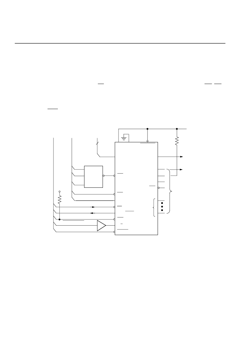
Peripheral Mode
Peripheral mode provides a simplified interface through which the device may be loaded byte-wide, as a processor
peripheral. Figure 23 shows the peripheral mode connections. Processor write cycles are decoded from the com-
mon assertion of the active-low write strobe (
WS
), and two active-low and one active-high chip selects (
CS0
,
CS1
,
CS2). If all of these signals are not available, the unused inputs should be driven to their respective active levels.
The FPGA will accept 1 byte of configuration data on the D[7:0] inputs for each selected processor write cycle.
Each byte of data is loaded into a buffer register. The FPGA generates a CCLK from the internal timing generator
and serializes the parallel input data for internal framing or for succeeding slaves on data out (DOUT). An output
HIGH on READY/
BUSY
pin indicates the completion of loading for each byte when the input register is ready for a
new byte. As with master modes, peripheral mode may also be used as a lead device for a daisy-chain of slave
devices.
Figure 23. Peripheral Mode
REPROGRAM
+5 V
ADDRESS
BUS
CONTROL
SIGNALS
ADDRESS
DECODE
LOGIC
8
GENERAL-
PURPOSE
USER I/O
OTHER
I/O PINS
LDC
HDC
M2
DOUT
CCLK
CS0
D[7:0]
CS1
CS2
WS
RDY/BUSY
INIT
D/P
RESET
D[7:0]
M0
M1
PWRDWN
*
*
+5 V
DATA
BUS
5 k
OC
5-3114(F)
相關(guān)PDF資料 |
PDF描述 |
|---|---|
| ATT3030-70H84I | Field-Programmable Gate Arrays |
| ATT3030-70J132I | Field-Programmable Gate Arrays |
| ATT3030-70J44I | Field-Programmable Gate Arrays |
| ATT3030-70J68I | Field-Programmable Gate Arrays |
| ATT3030-70J84I | Field-Programmable Gate Arrays |
相關(guān)代理商/技術(shù)參數(shù) |
參數(shù)描述 |
|---|---|
| ATT3030-70H84I | 制造商:未知廠家 制造商全稱:未知廠家 功能描述:Field-Programmable Gate Arrays |
| ATT3030-70J100 | 制造商:未知廠家 制造商全稱:未知廠家 功能描述:Field Programmable Gate Array (FPGA) |
| ATT3030-70J100I | 制造商:未知廠家 制造商全稱:未知廠家 功能描述:Field Programmable Gate Array (FPGA) |
| ATT3030-70J132I | 制造商:未知廠家 制造商全稱:未知廠家 功能描述:Field-Programmable Gate Arrays |
| ATT3030-70J44I | 制造商:未知廠家 制造商全稱:未知廠家 功能描述:Field-Programmable Gate Arrays |
發(fā)布緊急采購,3分鐘左右您將得到回復(fù)。