- 您現(xiàn)在的位置:買賣IC網(wǎng) > PDF目錄379698 > ATT3042-125M84I (Electronic Theatre Controls, Inc.) Field-Programmable Gate Arrays PDF資料下載
參數(shù)資料
| 型號: | ATT3042-125M84I |
| 廠商: | Electronic Theatre Controls, Inc. |
| 元件分類: | FPGA |
| 英文描述: | Field-Programmable Gate Arrays |
| 中文描述: | 現(xiàn)場可編程門陣列 |
| 文件頁數(shù): | 34/80頁 |
| 文件大小: | 528K |
| 代理商: | ATT3042-125M84I |
第1頁第2頁第3頁第4頁第5頁第6頁第7頁第8頁第9頁第10頁第11頁第12頁第13頁第14頁第15頁第16頁第17頁第18頁第19頁第20頁第21頁第22頁第23頁第24頁第25頁第26頁第27頁第28頁第29頁第30頁第31頁第32頁第33頁當前第34頁第35頁第36頁第37頁第38頁第39頁第40頁第41頁第42頁第43頁第44頁第45頁第46頁第47頁第48頁第49頁第50頁第51頁第52頁第53頁第54頁第55頁第56頁第57頁第58頁第59頁第60頁第61頁第62頁第63頁第64頁第65頁第66頁第67頁第68頁第69頁第70頁第71頁第72頁第73頁第74頁第75頁第76頁第77頁第78頁第79頁第80頁
Data Sheet
February 1997
ATT3000 Series Field-Programmable Gate Arrays
34
Lucent Technologies Inc.
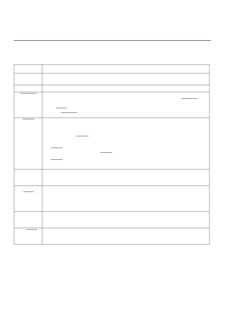
Pin Information
Table 4. Permanently Dedicated Pins
Symbol
Name/Description
V
CC
Two to eight (depending on package type) connections to the nominal +5 V supply voltage. All
must be connected.
GND
Two to eight (depending on package type) connections to ground. All must be connected.
PWRDWN
A low on this CMOS compatible input stops all internal activity to minimize V
CC
power, and puts
all output buffers in a high-impedance state; configuration is retained. When the
PWRDWN
pin
returns high, the device returns to operation with the same sequence of buffer enable and
DONE/
PROG
as at the completion of configuration. All internal storage elements are reset. If
not used,
PWRDWN
must be tied to V
CC
.
RESET
This is an active-low input which has three functions:
I
Prior to the start of configuration, a low input will delay the start of the configuration process.
An internal circuit senses the application of power and begins a minimal time-out cycle. When
the time-out and
RESET
are complete, the levels of the M lines are sampled and configuration
begins.
I
If
RESET
is asserted during a configuration, the FPGA is reinitialized and will restart the con-
figuration at the termination of
RESET
.
I
If
RESET
is asserted after configuration is complete, it will provide an asynchronous reset of all
IOB and CLB storage elements of the FPGA.
CCLK
Configuration Clock
. During configuration, this is an output of an FPGA in master mode or
peripheral mode. FPGAs in slave mode use it as a clock input. During a readback operation, it is
a clock input for the configuration data being filtered out.
DONE/
PROG
DONE Output
. Configurable as open drain with or without an internal pull-up resistor. At the
completion of configuration, the circuitry of the FPGA becomes active in a synchronous order,
and DONE may be programmed to occur one cycle before or after that occurs. Once configura-
tion is done, a high-to-low transition of this pin will cause an initialization of the FPGA and start a
reconfiguration.
M0/RTRIG
Mode 0
. This input, M1, and M2 are sampled before the start of configuration to establish the
configuration mode to be used. After configuration is complete, a low-to-high transition acts as a
read trigger to initiate a readback of configuration and storage-element data clocked by CCLK.
M1/
RDATA
Mode 1
. This input, M0, and M2 are sampled before the start of configuration to establish the
configuration mode to be used. After configuration is complete, this pin is the active-low output of
the readback data.
相關(guān)PDF資料 |
PDF描述 |
|---|---|
| ATT3042-125S132I | Field-Programmable Gate Arrays |
| ATT3042-50M132I | Field-Programmable Gate Arrays |
| ATT3042-50M44I | Field-Programmable Gate Arrays |
| ATT3042-50M68I | Field-Programmable Gate Arrays |
| ATT3042-50M84I | Field-Programmable Gate Arrays |
相關(guān)代理商/技術(shù)參數(shù) |
參數(shù)描述 |
|---|---|
| ATT3042-125N100 | 制造商:未知廠家 制造商全稱:未知廠家 功能描述:Field Programmable Gate Array (FPGA) |
| ATT3042-125N100M | 制造商:未知廠家 制造商全稱:未知廠家 功能描述:Field Programmable Gate Array (FPGA) |
| ATT3042-125R132M | 制造商:未知廠家 制造商全稱:未知廠家 功能描述:Field Programmable Gate Array (FPGA) |
| ATT3042-125R84M | 制造商:未知廠家 制造商全稱:未知廠家 功能描述:Field Programmable Gate Array (FPGA) |
| ATT3042-125S132I | 制造商:未知廠家 制造商全稱:未知廠家 功能描述:Field-Programmable Gate Arrays |
發(fā)布緊急采購,3分鐘左右您將得到回復。