- 您現(xiàn)在的位置:買賣IC網(wǎng) > PDF目錄379702 > AZ10EL89DR1 (Electronic Theatre Controls, Inc.) ECL/PECL Coaxial Cable Driver PDF資料下載
參數(shù)資料
| 型號(hào): | AZ10EL89DR1 |
| 廠商: | Electronic Theatre Controls, Inc. |
| 英文描述: | ECL/PECL Coaxial Cable Driver |
| 中文描述: | ECL / PECL的同軸電纜驅(qū)動(dòng)器 |
| 文件頁(yè)數(shù): | 2/4頁(yè) |
| 文件大小: | 134K |
| 代理商: | AZ10EL89DR1 |
AZ10EL89
October 2001 * REV - 0
www.azmicrotek.com
2
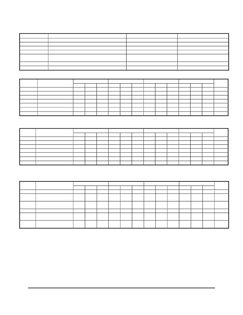
Absolute Maximum Ratings are those values beyond which device life may be impaired.
Symbol
Characteristic
V
CC
PECL Power Supply (V
EE
= 0V)
V
I
PECL Input Voltage (V
EE
= 0V)
V
EE
ECL Power Supply (V
CC
= 0V)
V
I
ECL Input Voltage (V
CC
= 0V)
Output Current
--- Continuous
--- Surge
T
A
Operating Temperature Range
T
STG
Storage Temperature Range
10K ECL DC Characteristics
(V
EE
= -4.2V to -5.7V, V
CC
= GND)
-40
°
C
Symbol
Characteristic
Min
Typ
V
OH
Output HIGH Voltage
1
-1230
V
OL
Output LOW Voltage
1
-2900
V
IH
Input HIGH Voltage
-1230
V
IL
Input LOW Voltage
-1950
I
IL
Input LOW Current
0.5
I
IH
Input HIGH Current
I
EE
Power Supply Current
23
1.
Each output is terminated through a 50
resistor to V
CC
– 3V.
10K PECL DC Characteristics
(V
EE
= GND, V
CC
= +5.0V)
-40
°
C
Symbol
Characteristic
Min
Typ
V
OH
Output HIGH Voltage
1,2
3770
V
OL
Output LOW Voltage
1,2
2100
V
IH
Input HIGH Voltage
1
3770
V
IL
Input LOW Voltage
1
3050
I
IL
Input LOW Current
0.5
I
IH
Input HIGH Current
I
EE
Power Supply Current
23
1.
For supply voltages other that 5.0V, use the ECL table values and ADD supply voltage value.
2.
Each output is terminated through a 50
resistor to V
CC
– 3V.
AC Characteristics
(V
EE
= -4.2V to -5.7V, V
CC
= GND or V
EE
= GND, V
CC
= +4.2V to +5.7V)
-40
°
C
Symbol
Characteristic
Min
Typ
Max
t
max
Maximum Toggle Rate
Propagation Delay
to Output
Within-Device Skew
1
Duty Cycle Skew
V
PP
(AC)
Minimum Input Swing
3
150
V
EE
+
2.5
Output Rise/Fall Times Q
(20% - 80%)
1.
Within-device skew defined as identical transitions on similar paths through a device.
2.
Duty cycle skew is the difference between a t
PLH
and t
PHL
propagation delay through a device.
3.
4.
The V
CMR
range is referenced to the most positive side of the differential input signal. Normal operation is obtained if the HIGH level falls within
the specified range and the peak-to-peak voltage lies between V
PP
(min) and 1V.
Rating
0 to +8.0
0 to +6.0
-8.0 to 0
-6.0 to 0
50
100
-40 to +85
-65 to +150
Unit
Vdc
Vdc
Vdc
Vdc
I
OUT
mA
°
C
°
C
0
°
C
Typ
23
25
°
C
Typ
23
85
°
C
Typ
23
Max
-980
-2580
-890
-1500
150
28
Min
-1180
-2950
-1170
-1950
0.5
Max
-940
-2570
-840
-1480
150
28
Min
-1130
-3000
-1130
-1950
0.5
Max
-900
-2560
-810
-1480
150
28
Min
-1060
-3050
-1060
-1950
0.5
Max
-810
-2510
-720
-1445
150
28
Unit
mV
mV
mV
mV
μ
A
μ
A
mA
0
°
C
Typ
23
25
°
C
Typ
23
85
°
C
Typ
23
Max
4020
2420
4110
3500
150
28
Min
3820
2050
3830
3050
0.5
Max
4060
2430
4160
3520
150
28
Min
3870
2000
3870
3050
0.5
Max
4100
2440
4190
3520
150
28
Min
3940
1950
3940
3050
0.5
Max
4190
2490
4280
3555
150
28
Unit
mV
mV
mV
mV
μ
A
μ
A
mA
0
°
C
Typ
25
°
C
Typ
1.5
85
°
C
Typ
Min
Max
Min
Max
Min
Max
Unit
Gb/s
t
PLH /
t
PHL
200
340
480
250
340
430
260
350
440
310
400
490
ps
t
SKEW
5
20
5
20
5
20
5
20
ps
150
V
EE
+
2.5
150
V
EE
+
2.5
150
V
EE
+
2.5
mV
V
CMR
Common Mode Range
4
V
CC
-
0.4
V
CC
-
0.4
V
CC
-
0.4
V
CC
-
0.4
V
t
r
/ t
f
205
455
205
455
205
455
205
455
ps
V
PP
is the minimum peak-to-peak differential input swing for which AC parameters guaranteed. The device has a DC gain of
≈
40.
相關(guān)PDF資料 |
PDF描述 |
|---|---|
| AZ10EL89 | ECL/PECL Coaxial Cable Driver |
| AZ10EL89D | ECL/PECL Coaxial Cable Driver |
| AZ10EL89DR2 | ECL/PECL Coaxial Cable Driver |
| AZ2101-1A-5D | MINIATURE POWER RELAY |
| AZ2100-1A-110D | MINIATURE POWER RELAY |
相關(guān)代理商/技術(shù)參數(shù) |
參數(shù)描述 |
|---|---|
| AZ-1100 | 制造商:Thomas & Betts 功能描述:Tapes Non Adhesive Black/Yellow Vinyl Cloth 27.4m |
| AZ1117 | 制造商:BCDSEMI 制造商全稱:BCD Semiconductor Manufacturing Limited 功能描述:1A LOW DROPOUT LINEAR REGULATOR |
| AZ1117_12 | 制造商:BCDSEMI 制造商全稱:BCD Semiconductor Manufacturing Limited 功能描述:1A LOW DROPOUT LINEAR REGULATOR |
| AZ1117_13 | 制造商:BCDSEMI 制造商全稱:BCD Semiconductor Manufacturing Limited 功能描述:1A LOW DROPOUT LINEAR REGULATOR |
| AZ1117B | 制造商:BCDSEMI 制造商全稱:BCD Semiconductor Manufacturing Limited 功能描述:600mA LOW DROPOUT LINEAR REGULATOR |
發(fā)布緊急采購(gòu),3分鐘左右您將得到回復(fù)。