- 您現(xiàn)在的位置:買賣IC網(wǎng) > PDF目錄295137 > BA08CC0FP-TR 8 V FIXED POSITIVE LDO REGULATOR, 0.5 V DROPOUT, PSSO3 PDF資料下載
參數(shù)資料
| 型號(hào): | BA08CC0FP-TR |
| 元件分類: | 固定正電壓?jiǎn)温份敵鯨DO穩(wěn)壓器 |
| 英文描述: | 8 V FIXED POSITIVE LDO REGULATOR, 0.5 V DROPOUT, PSSO3 |
| 封裝: | LEAD FREE, TO-252, 3 PIN |
| 文件頁(yè)數(shù): | 7/9頁(yè) |
| 文件大?。?/td> | 1047K |
| 代理商: | BA08CC0FP-TR |

7/8
●
Other Points of Caution
1)Protection Circuits
Over-current Protection Circuit
A built-in over-current protection circuit corresponding to the current capacity prevents the destruction of the IC when there
are load shorts. This protection circuit is a “7”-shaped current control circuit that is designed such that the current is restricted
and does not latch even when a large current momentarily flows through the system with a high-capacitance capacitor.
However, while this protection circuit is effective for the prevention of destruction due to unexpected accidents, it is not
suitable for continuous operation or transient use. Please be aware when creating thermal designs that the overcurrent
protection circuit has negative current capacity characteristics with regard to temperature (Refer to Figs.4 and 16).
Thermal Shutdown Circuit (Thermal Protection)
This system has a built-in temperature protection circuit for the purpose of protecting the IC from thermal damage. As shown
above, this must be used within the range of acceptable loss, but if the acceptable loss happens to be continuously exceeded,
the chip temperature Tj increases, causing the temperature protection circuit to operate.
When the thermal shutdown circuit operates, the operation of the circuit is suspended. The circuit resumes operation
immediately after the chip temperature Tj decreases, so the output repeats the ON and OFF states (Please refer to Figs.12
and 24 for the temperatures at which the temperature protection circuit operates).
There are cases in which the IC is destroyed due to thermal runaway when it is left in the overloaded state. Be sure to avoid
leaving the IC in the overloaded state.
Reverse Current
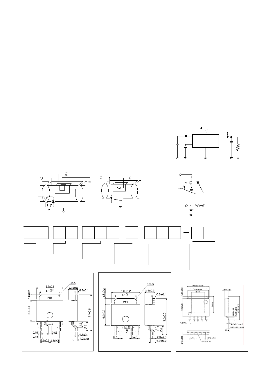
In order to prevent the destruction of the IC when a reverse current flows through the IC, it is recommended that a diode
be placed between the Vcc and Vo and a pathway be created so that the current can escape (Refer to Fig.35).
2) This IC is bipolar IC that has a P-board (substrate) and P+ isolation layer
between each devise, as shown in Fig.36. A P-N junction is formed between
this P-layer and the N-layer of each device, and the P-N junction operates as a
parasitic diode when the electric potential relationship is GND> Terminal A,
GND> Terminal B, while it operates as a parasitic transistor when the electric
potential relationship is Terminal B GND> Terminal A. Parasitic devices are
structurally inevitable in the IC. The operation of parasitic devices induces
mutual interference between circuits, causing malfunctions and eventually the
destruction of the IC. It is necessary to be careful not to use the IC in ways that
would cause parasitic elements to operate. For example, applying a voltage
that is lower than the GND (P-board) to the input terminal.
Fig. 37: Example of the basic structure of a bipolar IC
●Part Number Selection
GND
N
P
N
P+
Parasitic element
or transistor
(Pin B)
B
E
Transistor (NPN)
N
P
N
GND
O
(Pin A)
GND
N
P+
Resistor
Parasitic element
P
N
P
P+
N
(Pin A)
Parasitic element
or transistor
(Pin B)
GND
C
B
E
Parasitic element
GND
Fig. 36:Bypass diode
OUT
Vcc
CTL
GND
Reverse current
ROHM
model name
Output
voltage
Current capacity
CC0 : 1A
DD0 : 2A
Shutdown switch
W : With switch
None : Without
switch
T :
F P :
HFP :
B
3 3 D D
W
H
0
A
P
E 2
F
Package specification
TR : Embossed taping(HRP5)
E2 : Embossed taping(TO252-3,5)
None : Tube container
V5 :Foaming(V5 only)
Package
TO220-3,5
TO252-3,5
HRP5
(Unit:mm)
TO252-3
(Unit:mm)
TO252-5
(Unit:mm)
HRP5
相關(guān)PDF資料 |
PDF描述 |
|---|---|
| BA15DD0T-E2 | 1.5 V FIXED POSITIVE LDO REGULATOR, 0.7 V DROPOUT, SFM3 |
| BA15DD0T-TR | 1.5 V FIXED POSITIVE LDO REGULATOR, 0.7 V DROPOUT, SFM3 |
| BA15DD0WHFP-E2 | 1.5 V FIXED POSITIVE LDO REGULATOR, 0.7 V DROPOUT, PSSO5 |
| BA15DD0WT-E2 | 1.5 V FIXED POSITIVE LDO REGULATOR, 0.7 V DROPOUT, SFM5 |
| BA15DD0WT-TR | 1.5 V FIXED POSITIVE LDO REGULATOR, 0.7 V DROPOUT, SFM5 |
相關(guān)代理商/技術(shù)參數(shù) |
參數(shù)描述 |
|---|---|
| BA08CC0T | 功能描述:低壓差穩(wěn)壓器 - LDO REG 1A 8V RoHS:否 制造商:Texas Instruments 最大輸入電壓:36 V 輸出電壓:1.4 V to 20.5 V 回動(dòng)電壓(最大值):307 mV 輸出電流:1 A 負(fù)載調(diào)節(jié):0.3 % 輸出端數(shù)量: 輸出類型:Fixed 最大工作溫度:+ 125 C 安裝風(fēng)格:SMD/SMT 封裝 / 箱體:VQFN-20 |
| BA08CC0WFP | 制造商:ROHM 制造商全稱:Rohm 功能描述:Standard Fixed Output LDO Regulators |
| BA08CC0WFP-E2 | 功能描述:低壓差穩(wěn)壓器 - LDO REG 1A 8V RoHS:否 制造商:Texas Instruments 最大輸入電壓:36 V 輸出電壓:1.4 V to 20.5 V 回動(dòng)電壓(最大值):307 mV 輸出電流:1 A 負(fù)載調(diào)節(jié):0.3 % 輸出端數(shù)量: 輸出類型:Fixed 最大工作溫度:+ 125 C 安裝風(fēng)格:SMD/SMT 封裝 / 箱體:VQFN-20 |
| BA08CC0WT | 功能描述:低壓差穩(wěn)壓器 - LDO REG 1A 8V RoHS:否 制造商:Texas Instruments 最大輸入電壓:36 V 輸出電壓:1.4 V to 20.5 V 回動(dòng)電壓(最大值):307 mV 輸出電流:1 A 負(fù)載調(diào)節(jié):0.3 % 輸出端數(shù)量: 輸出類型:Fixed 最大工作溫度:+ 125 C 安裝風(fēng)格:SMD/SMT 封裝 / 箱體:VQFN-20 |
| BA08CC0WT-V5 | 功能描述:低壓差穩(wěn)壓器 - LDO LDO REG 8V 1A 5PIN RoHS:否 制造商:Texas Instruments 最大輸入電壓:36 V 輸出電壓:1.4 V to 20.5 V 回動(dòng)電壓(最大值):307 mV 輸出電流:1 A 負(fù)載調(diào)節(jié):0.3 % 輸出端數(shù)量: 輸出類型:Fixed 最大工作溫度:+ 125 C 安裝風(fēng)格:SMD/SMT 封裝 / 箱體:VQFN-20 |
發(fā)布緊急采購(gòu),3分鐘左右您將得到回復(fù)。