- 您現(xiàn)在的位置:買賣IC網(wǎng) > PDF目錄223495 > C-13-622C-F-SLC-G5 FIBER OPTIC TRANSCEIVER, 1274-1356nm, 622Mbps(Tx), 622Mbps(Rx), LC CONNECTOR PDF資料下載
參數(shù)資料
| 型號(hào): | C-13-622C-F-SLC-G5 |
| 元件分類: | 光收發(fā) |
| 英文描述: | FIBER OPTIC TRANSCEIVER, 1274-1356nm, 622Mbps(Tx), 622Mbps(Rx), LC CONNECTOR |
| 封裝: | ROHS COMPLIANT PACKAGE |
| 文件頁數(shù): | 5/9頁 |
| 文件大小: | 699K |
| 代理商: | C-13-622C-F-SLC-G5 |

5
622 Mbps Single Mode SFF LC Transceiver
C-13-622(C)-F-SLC(A)(-55)-G5
20550 Nordhoff St. Chatsworth, CA 91311 tel: 818.773.9044 fax: 818.576.9486
9F, No 81, Shui Lee Rd. Hsinchu, Taiwan, R.O.C. tel: 886.3.5169222 fax: 886.3.5169213
LUMNDS1932-Aug0508
Rev A.0
LUMINENTOIC.COM
Printed Circuit Board Layout Consideration
A ber-optic receiver employs a very high gain, wide bandwidth transimpedance amplier. This amplier detects and amplies signals
that are only tens of nA in amplitude when the receiver is operating near it’s limit. Any unwanted signal current that couples into the receiver
circuitry causes a decrease in the receiver’s sensitivity and can also degrade the performance of the receiver’s signal detect (SD) circuit. To minimize
the coupling of unwanted noise into the receiver, careful attention must be given to the printed circuit board.
At a minimum, a double-sided printed circuit board(PCB) with a large component side ground plane beneath the transceiver must be
used. In applications that include many other high speed devices, a multi-layer PCB is highly recommended. This permits the placement of power
and ground on separate layers, wich allows them to be isolated from the signal lines. Multilayer construction also permits the routing of signal
traces away from high level, high speed sinal lines. To minimize the possibility of coupling noise into the receiver section, high level, high speed
signals such as transmitter inputs and clock lines should be routed as far away as possible from the receiver pins.
Noise that couples into the receiver through the power supply pins can also degrade performance. It is recommended that a pi lter be
used in both transmitter and receiver power supplies.
EMI and ESC Consideration
OIC transceivers offer a metalized plastic case and a special chassis grounding clip. As shown in the drawing, this clip connects the
module case to chassis ground then installs ush through the panel cutout. This way, the grounding clip brushes the edge of the cutout in order
to make a proper contact. The use of a grounding clip also provides increased electrostatic protection and helps reduce radiated emission from the
module or the host circuit board through the chassis faceplate. The attaching posts are at case potential and may be connected to chassis ground.
They should not be connected to circuit ground.
Plastic optical subassemblies are used to further reduce the possibility of radiated emission by eliminating the metal from the
transmitter and receiver diode housings, which extend into connector space. By providing a non-metal receptacle for the optical cable ferrule, the
gigabit speed RF electrical signal is isolated from the connector area thus preventing radiated energy leakage from these surfaces to the outside of
the panel.
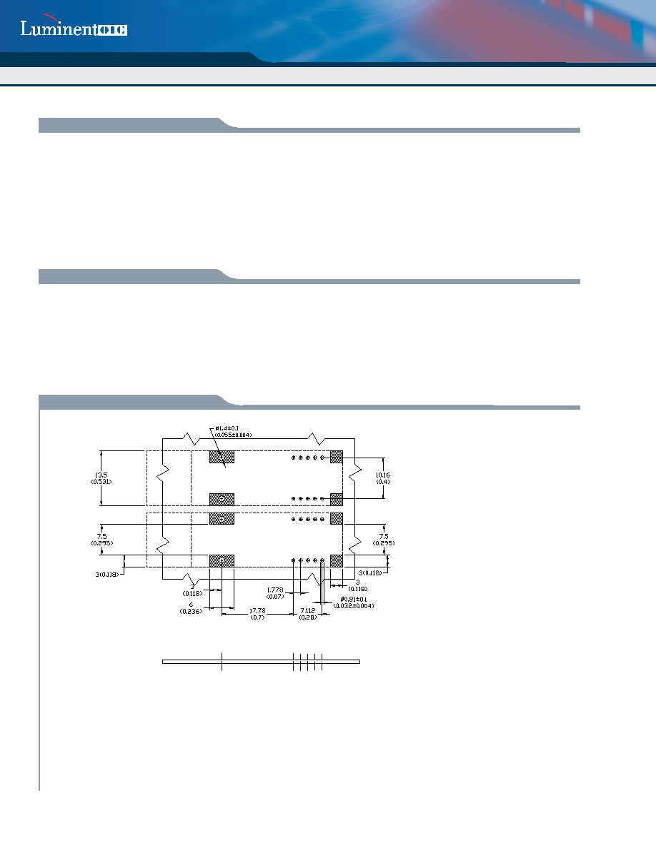
Recommended Board Layout Hole Pattern
1.THIS FIGURE DESCRIBE THE RECOMMAND CIRCUIT BOARD LAYOUT FOR THE SFF TRANSCEIVER.
2.THE HATCHED AREAS ARE KEEP-OUT AREAS RESERVED FOR HOUSING STANDOFF. NO METAL
TRACES OR GROUND CONNECTION IN KEEP-OUT AREAS.
3.THE MOUNTING STUDS SHOULD BE SOLDERED TO CHASSIS GROUND FOR MECHANICAL INTEGRITY.
DIMENSION IN MILLIMETER (INCHES)
NOTES:
相關(guān)PDF資料 |
PDF描述 |
|---|---|
| C-13-622C-F-SLCA-G5 | FIBER OPTIC TRANSCEIVER, 1274-1356nm, 622Mbps(Tx), 622Mbps(Rx), LC CONNECTOR |
| C-13-622-F-SLC-55-G5 | FIBER OPTIC TRANSCEIVER, 1274-1356nm, 622Mbps(Tx), 622Mbps(Rx), LC CONNECTOR |
| C-13-622C-F-SLCA-55-G5 | FIBER OPTIC TRANSCEIVER, 1274-1356nm, 622Mbps(Tx), 622Mbps(Rx), LC CONNECTOR |
| C-13-622-F-SLCA-55-G5 | FIBER OPTIC TRANSCEIVER, 1274-1356nm, 622Mbps(Tx), 622Mbps(Rx), LC CONNECTOR |
| C-13-622-T-SFC | FIBER OPTIC TRANSCEIVER, 1274-1356nm, 622Mbps(Tx), 622Mbps(Rx), THROUGH HOLE MOUNT, FC CONNECTOR |
相關(guān)代理商/技術(shù)參數(shù) |
參數(shù)描述 |
|---|---|
| C-13-622C-T3-SSC4 | 制造商:SOURCE 制造商全稱:Source Photonics, Inc. 功能描述:622 Mbps Single Mode Transceiver |
| C-13-622C-T3-SSC4A | 制造商:SOURCE 制造商全稱:Source Photonics, Inc. 功能描述:622 Mbps Single Mode Transceiver |
| C-13-622C-T3-SSC4A-G5 | 制造商:SOURCE 制造商全稱:Source Photonics, Inc. 功能描述:622 Mbps Single Mode Transceiver |
| C-13-622C-T3-SSC4B | 制造商:SOURCE 制造商全稱:Source Photonics, Inc. 功能描述:622 Mbps Single Mode Transceiver |
| C-13-622C-T3-SSC4B-G5 | 制造商:SOURCE 制造商全稱:Source Photonics, Inc. 功能描述:622 Mbps Single Mode Transceiver |
發(fā)布緊急采購,3分鐘左右您將得到回復(fù)。