- 您現(xiàn)在的位置:買賣IC網(wǎng) > PDF目錄378429 > C165 (INFINEON TECHNOLOGIES AG) 16-Bit Single-Chip Microcontroller PDF資料下載
參數(shù)資料
| 型號: | C165 |
| 廠商: | INFINEON TECHNOLOGIES AG |
| 英文描述: | 16-Bit Single-Chip Microcontroller |
| 中文描述: | 16位單片機 |
| 文件頁數(shù): | 11/77頁 |
| 文件大小: | 1371K |
| 代理商: | C165 |
第1頁第2頁第3頁第4頁第5頁第6頁第7頁第8頁第9頁第10頁當前第11頁第12頁第13頁第14頁第15頁第16頁第17頁第18頁第19頁第20頁第21頁第22頁第23頁第24頁第25頁第26頁第27頁第28頁第29頁第30頁第31頁第32頁第33頁第34頁第35頁第36頁第37頁第38頁第39頁第40頁第41頁第42頁第43頁第44頁第45頁第46頁第47頁第48頁第49頁第50頁第51頁第52頁第53頁第54頁第55頁第56頁第57頁第58頁第59頁第60頁第61頁第62頁第63頁第64頁第65頁第66頁第67頁第68頁第69頁第70頁第71頁第72頁第73頁第74頁第75頁第76頁第77頁
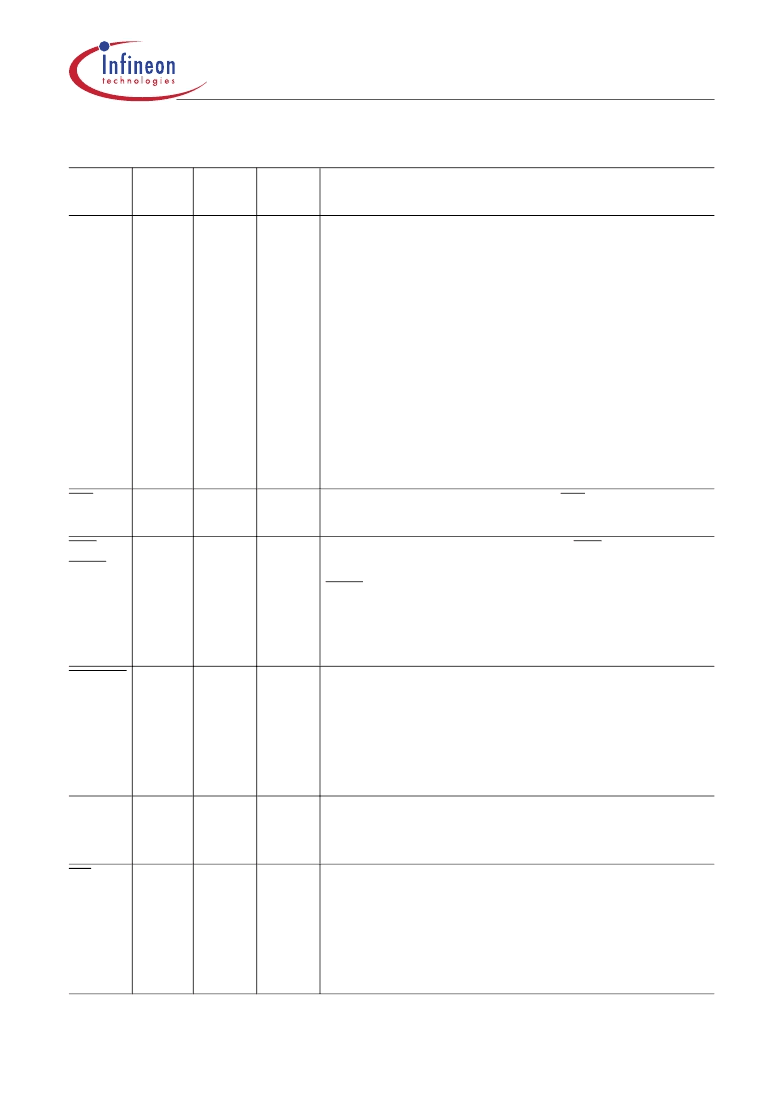
C165
Data Sheet
7
V2.0, 2000-12
P4
P4.0
P4.1
P4.2
P4.3
P4.4
P4.5
P4.6
P4.7
RD
23
24
25
26
29
30
31
32
33
25
26
27
28
31
32
33
34
35
IO
O
O
O
O
O
O
O
O
O
Port 4 is an 8-bit bidirectional I/O port. It is bit-wise
programmable for input or output via direction bits.
For a pin configured as input, the output driver is put
into high-impedance state. Port 4 can be used to
output the segment address lines:
A16
Least Significant Segment Address Line
A17
Segment Address Line
A18
Segment Address Line
A19
Segment Address Line
A20
Segment Address Line
A21
Segment Address Line
A22
Segment Address Line
A23
Most Significant Segment Address Line
External Memory Read Strobe. RD is activated for
every external instruction or data read access.
External Memory Write Strobe. In WR-mode this pin
is activated for every external data write access. In
WRL-mode this pin is activated for low byte data
write accesses on a 16-bit bus, and for every data
write access on an 8-bit bus. See WRCFG in register
SYSCON for mode selection.
Ready Input. When the Ready function is enabled, a
high level at this pin during an external memory
access will force the insertion of memory cycle
waitstates until the pin returns to a low level.
An internal pullup device holds this pin high when
nothing is driving it.
Address Latch Enable Output. Can be used for
latching the address into external memory or an
address latch in the multiplexed bus modes.
External Access Enable pin. A low level at this pin
during and after Reset forces the C165 to begin
instruction execution out of external memory. A high
level forces execution out of the internal program
memory.
“ROMless” versions must have this pin tied to ‘0’.
WR/
WRL
34
36
O
READY 35
37
I
ALE
36
38
O
EA
37
39
I
Table 2
Symbol Pin Nr
Pin Definitions and Functions
(cont’d)
Pin Nr
MQFP
Outp.
TQFP
Input
Function
相關(guān)PDF資料 |
PDF描述 |
|---|---|
| C165 | C16x-Family of High-Performance CMOS 16-Bit Microcontrollers |
| C166 | 8-Bit Microcontroller(8位微控制器) |
| C1676 | Approved for use with GlobeSpan HDSL2 Chip Set Meets the requirements of IEC60950 for supplementary insulation, 250V working voltage |
| C167CR-16F | 16-Bit CMOS Single-Chip Microcontroller with 128KByte Flash EPROM |
| C167CR-16RM | 16-Bit CMOS Single-Chip Microcontrollers |
相關(guān)代理商/技術(shù)參數(shù) |
參數(shù)描述 |
|---|---|
| C165_96 | 制造商:INFINEON 制造商全稱:Infineon Technologies AG 功能描述:16-Bit CMOS Single-Chip Microcontrollers |
| C-165034-EE | 制造商:MACOM 制造商全稱:Tyco Electronics 功能描述:None |
| C-165051-10-9 | 制造商:TE Connectivity 功能描述:4-1200610-8,A73618-000 |
| C16550-000 | 制造商:TE Connectivity 功能描述: |
| C1656 | 制造商:COEV 功能描述: |
發(fā)布緊急采購,3分鐘左右您將得到回復。