- 您現(xiàn)在的位置:買賣IC網(wǎng) > PDF目錄378432 > C515A (SIEMENS AG) 8-Bit CMOS Microcontroller PDF資料下載
參數(shù)資料
| 型號: | C515A |
| 廠商: | SIEMENS AG |
| 元件分類: | 8位微控制器 |
| 英文描述: | 8-Bit CMOS Microcontroller |
| 中文描述: | 8位CMOS微控制器 |
| 文件頁數(shù): | 44/58頁 |
| 文件大?。?/td> | 634K |
| 代理商: | C515A |
第1頁第2頁第3頁第4頁第5頁第6頁第7頁第8頁第9頁第10頁第11頁第12頁第13頁第14頁第15頁第16頁第17頁第18頁第19頁第20頁第21頁第22頁第23頁第24頁第25頁第26頁第27頁第28頁第29頁第30頁第31頁第32頁第33頁第34頁第35頁第36頁第37頁第38頁第39頁第40頁第41頁第42頁第43頁當前第44頁第45頁第46頁第47頁第48頁第49頁第50頁第51頁第52頁第53頁第54頁第55頁第56頁第57頁第58頁
C515A
Semiconductor Group
44
1997-10-01
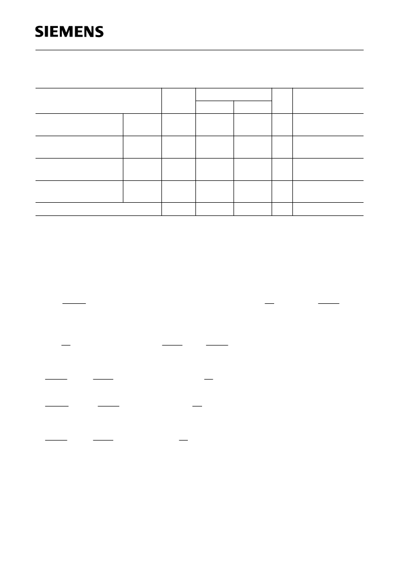
Power Supply Current
Notes:
1) Capacitive loading on ports 0 and 2 may cause spurious noise pulses to be superimposed on the
V
OL
of ALE
and port 3. The noise is due to external bus capacitance discharging into the port 0 and port 2 pins when these
pins make 1-to-0 transitions during bus operation. In the worst case (capacitive loading > 100 pF), the noise
pulse on ALE line may exceed 0.8 V. In such cases it may be desirable to qualify ALE with a schmitt-trigger,
or use an address latch with a schmitt-trigger strobe input.
2) Capacitive loading on ports 0 and 2 may cause the
V
OH
on ALE and PSEN to momentarily fall below the
0.9
V
CC
specification when the address lines are stabilizing.
3)
I
PD
(software power-down mode) is measured under following conditions:
EA = RESET = Port 0 = Port 6 =
V
CC
; XTAL1 = N.C.; XTAL2 =
V
SS
; PE/SWD =
V
SS
;
HWPD =
V
CC
;
V
AGND
=
V
SS
;
V
AREF
=
V
CC
; all other pins are disconnected.
I
PD
(hardware power-down mode): independent from any particular pin connection.
4)
I
CC
(active mode) is measured with:
XTAL2 driven with
t
CLCH
,
t
CHCL
= 5 ns ,
V
IL
=
V
SS
+ 0.5 V,
V
IH
=
V
CC
– 0.5 V; XTAL1 = N.C.;
EA = PE/SWD = Port 0 = Port 6 =
V
CC
; HWPD =
V
CC
;
RESET =
V
SS
;
all other pins are disconnected.
I
CC
would be slightly higher if a crystal oscillator is used (appr. 1 mA).
5)
I
CC
(idle mode) is measured with all output pins disconnected and with all peripherals disabled;
XTAL2 driven with
t
CLCH
,
t
CHCL
= 5 ns,
V
IL
=
V
SS
+ 0.5 V,
V
IH
=
V
CC
– 0.5 V; XTAL1 = N.C.;
RESET =
V
CC
; HWPD = Port 0 = Port 6 =
V
CC
; EA = PE/SWD =
V
SS
; all other pins are disconnected;
6)
I
CC
(active mode with slow-down mode) is measured with all output pins disconnected and with all peripherals
disabled; XTAL2 driven with
t
CLCH
,
t
CHCL
= 5 ns,
V
IL
=
V
SS
+ 0.5 V,
V
IH
=
V
CC
– 0.5 V; XTAL1 = N.C.;
RESET =
V
CC
; HWPD = Port 6 =
V
CC
; EA = PE/SWD =
V
SS
; all other pins are disconnected; the
microcontroller is put into slow-down mode by software;
7)
I
CC
(idle mode with slow-down mode) is measured with all output pins disconnected and with all peripherals
disabled; XTAL2 driven with
t
CLCH
,
t
CHCL
= 5 ns,
V
IL
=
V
SS
+ 0.5 V,
V
IH
=
V
CC
– 0.5 V; XTAL1 = N.C.;
RESET =
V
CC
; HWPD = Port 6 =
V
CC
; EA = PE/SWD =
V
SS
; all other pins are disconnected;
the microcontroller is put into idle mode with slow-down mode enabled by software;
8) Overload conditions occur if the standard operating conditions are exceeded, i.e. the voltage on any pin
exceeds the specified range (i.e.
V
OV
>
V
CC
+ 0.5 V or
V
OV
<
V
SS
- 0.5 V). The supply voltage
V
CC
and
V
SS
must
remain within the specified limits. The absolute sum of input currents on all port pins may not exceed 50 mA.
9) Not 100% tested, guaranteed by design characterization
10)The typical
I
CC
values are periodically measured at
T
A
= +25 C and
V
CC
= 5 V but not 100% tested.
11)The maximum
I
CC
values are measured under worst case conditions (
T
A
= 0 C or -40 C and
V
CC
= 5.5 V)
Parameter
Symbol
Limit Values
Unit Test Condition
typ.
10)
max.
11)
Active mode
18 MHz
24 MHz
I
CC
I
CC
I
CC
I
CC
I
CC
I
CC
I
CC
I
CC
I
PD
16.9
21.7
23.1
29.4
mA
mA
4)
Idle mode
18 MHz
24 MHz
8.5
11.0
12.1
15.0
mA
mA
5)
Active mode with
slow-down enabled
18 MHz
24 MHz
5.6
6.6
8.0
9.6
mA
mA
6)
Active mode with
slow-down enabled
18 MHz
24 MHz
3.0
3.3
4.1
4.7
mA
mA
μ
A
7)
Power-down mode
10
50
V
CC
= 2
…
5.5 V
3)
相關PDF資料 |
PDF描述 |
|---|---|
| C515C | 8-bit Microcontroller with 2/4/8K Bytes In-System Programmable Flash |
| C515C-8EM | RW-D Series - Econoline Regulated DC-DC Converters; Input Voltage (Vdc): 48V; Output Voltage (Vdc): 05V; Power: 2W; DIP24 Low Profile Package; Dual Ouputs from a Single Supply; 2:1 Wide Range Voltage Input; 3kVDC Isolation; UL94V-0 Package Material; Continuous Short Circuit Protection; Low profile 7mm Height; Approved for Medical Applications; Efficiency to 85% |
| C515C-8RM | RW-S Series - Econoline Regulated DC-DC Converters; Input Voltage (Vdc): 48V; Output Voltage (Vdc): 05V; Power: 2W; DIP24 Low Profile Miniature Package; 1kVDC Isolation; Feedback Regulated Output; 2:1 Wide Range Voltage Input; Continuous Short Circuit Protection; Less than 7mm Height; SMD Pinning Option; Efficiency to 87% |
| C515C-LM | 8-bit Microcontroller with 2/4/8K Bytes In-System Programmable Flash |
| C515C | 8-Bit CMOS Microcontroller |
相關代理商/技術參數(shù) |
參數(shù)描述 |
|---|---|
| C515A_9708 | 制造商:INFINEON 制造商全稱:Infineon Technologies AG 功能描述:8-Bit CMOS Microcontroller |
| C515C | 制造商:INFINEON 制造商全稱:Infineon Technologies AG 功能描述:8-Bit Single-Chip Microcontroller |
| C515C_9711 | 制造商:INFINEON 制造商全稱:Infineon Technologies AG 功能描述:8-Bit CMOS Microcontroller |
| C515C-8E | 制造商:INFINEON 制造商全稱:Infineon Technologies AG 功能描述:8-Bit CMOS Microcontroller |
| C515C-8EM | 制造商:INFINEON 制造商全稱:Infineon Technologies AG 功能描述:8-Bit Single-Chip Microcontroller |
發(fā)布緊急采購,3分鐘左右您將得到回復。