- 您現(xiàn)在的位置:買賣IC網(wǎng) > PDF目錄295214 > CAT25C64Y20I 8K X 8 SPI BUS SERIAL EEPROM, PDSO20 PDF資料下載
參數(shù)資料
| 型號: | CAT25C64Y20I |
| 元件分類: | PROM |
| 英文描述: | 8K X 8 SPI BUS SERIAL EEPROM, PDSO20 |
| 封裝: | LEAD FREE AND HALOGEN FREE, TSSOP-20 |
| 文件頁數(shù): | 9/11頁 |
| 文件大?。?/td> | 69K |
| 代理商: | CAT25C64Y20I |

7
CAT25C32/64
Doc. No. 1001, Rev. G
READ Sequence
The part is selected by pulling
CS low. The 8-bit read
instruction is transmitted to the CAT25C32/64, fol-
lowed by the 16-bit address(the three Most Significant
Bits are don’t care for 25C64 and four most significant
bits are don't care for 25C32).
After the correct read instruction and address are sent,
the data stored in the memory at the selected address
is shifted out on the SO pin. The data stored in the
memory at the next address can be read sequentially
by continuing to provide clock pulses. The internal
address pointer is automatically incremented to the
next higher address after each byte of data is shifted
out. When the highest address (1FFFh for 25C64 and
FFFh for 25C32) is reached, the address counter rolls
over to 0000h allowing the read cycle to be continued
indefinitely. The readoperation is terminated by pulling
the
CS high.
To read the status register, RDSR instruction should be
sent. The contents of the status register are shifted out on
the SO line. The status register may be read at any time
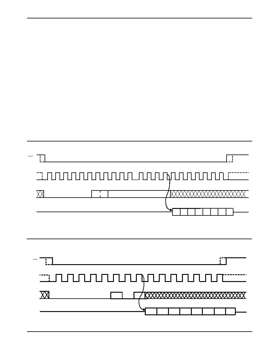
even during a write cycle. Read sequece is illustrated in
Figure 4. Reading status register is illustrated in Figure 5.
WRITE Sequence
The CAT25C32/64 powers up in a Write Disable state. Prior
to any write instructions, the WREN instruction must be
sent to CAT25C32/64. The device goes into Write enable
state by pulling the
CS low and then clocking the WREN
instruction into CAT25C32/64. The
CS must be brought
high after the WREN instruction to enable writes to the
device. If the write operation is initiated immediately after
the WREN instruction without
CS being brought high, the
data will not be written to thearray because the write enable
latch will not have been properly set. Also, for a successful
write operation the address of the memory location(s) to be
programmed must be outside the protected address field
location selected by the block protection level.
Figure 4. Read Instruction Timing
Figure 5. RDSR Instruction Timing
Note: Dashed Line= mode (1, 1) — — — —
SK
SI
SO
0000001
1
BYTE ADDRESS*
0123456789
10
20
21
22
23
24
25
26
27
28
29
30
7
6
5
4
3
2
1
0
*Please check the instruction set table for address
CS
OPCODE
DATA OUT
MSB
HIGH IMPEDANCE
0
1
2
345
67
8
10
911
12
13
14
SCK
SI
DATA OUT
MSB
HIGH IMPEDANCE
OPCODE
SO
7
6
5
4
3
2
1
0
CS
00
0
00
1
0
1
相關(guān)PDF資料 |
PDF描述 |
|---|---|
| CAT28C65BHFJ-15TE13 | 8K X 8 EEPROM 5V, 150 ns, PDSO28 |
| CAT28C65BHFKI-12TE7 | 8K X 8 EEPROM 5V, 120 ns, PDSO28 |
| CAT28C65BHFT13I-15TE7 | 8K X 8 EEPROM 5V, 150 ns, PDSO28 |
| CAT28C65BHT14-20TE7 | 8K X 8 EEPROM 5V, 200 ns, PDSO32 |
| CAT28F001NI-90T | 128K X 8 FLASH 12V PROM, 90 ns, PQCC32 |
相關(guān)代理商/技術(shù)參數(shù) |
參數(shù)描述 |
|---|---|
| CAT25C64Y20I-1.8 | 功能描述:電可擦除可編程只讀存儲器 (8kx8) 64K 1.8-6.0 RoHS:否 制造商:Atmel 存儲容量:2 Kbit 組織:256 B x 8 數(shù)據(jù)保留:100 yr 最大時鐘頻率:1000 KHz 最大工作電流:6 uA 工作電源電壓:1.7 V to 5.5 V 最大工作溫度:+ 85 C 安裝風(fēng)格:SMD/SMT 封裝 / 箱體:SOIC-8 |
| CAT25C65L | 功能描述:電可擦除可編程只讀存儲器 (8kx8) 64K 2.5-6.0 RoHS:否 制造商:Atmel 存儲容量:2 Kbit 組織:256 B x 8 數(shù)據(jù)保留:100 yr 最大時鐘頻率:1000 KHz 最大工作電流:6 uA 工作電源電壓:1.7 V to 5.5 V 最大工作溫度:+ 85 C 安裝風(fēng)格:SMD/SMT 封裝 / 箱體:SOIC-8 |
| CAT25C65L-1.8 | 功能描述:電可擦除可編程只讀存儲器 (8kx8) 64K 1.8-6.0 RoHS:否 制造商:Atmel 存儲容量:2 Kbit 組織:256 B x 8 數(shù)據(jù)保留:100 yr 最大時鐘頻率:1000 KHz 最大工作電流:6 uA 工作電源電壓:1.7 V to 5.5 V 最大工作溫度:+ 85 C 安裝風(fēng)格:SMD/SMT 封裝 / 箱體:SOIC-8 |
| CAT25C65LA | 功能描述:電可擦除可編程只讀存儲器 (8kx8) 64K 2.5-6.0 RoHS:否 制造商:Atmel 存儲容量:2 Kbit 組織:256 B x 8 數(shù)據(jù)保留:100 yr 最大時鐘頻率:1000 KHz 最大工作電流:6 uA 工作電源電壓:1.7 V to 5.5 V 最大工作溫度:+ 85 C 安裝風(fēng)格:SMD/SMT 封裝 / 箱體:SOIC-8 |
| CAT25C65LI | 功能描述:電可擦除可編程只讀存儲器 (8kx8) 64K 2.5-6.0 RoHS:否 制造商:Atmel 存儲容量:2 Kbit 組織:256 B x 8 數(shù)據(jù)保留:100 yr 最大時鐘頻率:1000 KHz 最大工作電流:6 uA 工作電源電壓:1.7 V to 5.5 V 最大工作溫度:+ 85 C 安裝風(fēng)格:SMD/SMT 封裝 / 箱體:SOIC-8 |
發(fā)布緊急采購,3分鐘左右您將得到回復(fù)。