- 您現(xiàn)在的位置:買賣IC網(wǎng) > PDF目錄384223 > CM3718C Low Noise PWM Step-Down Regulator |Battery Management ICs PDF資料下載
參數(shù)資料
| 型號(hào): | CM3718C |
| 英文描述: | Low Noise PWM Step-Down Regulator |Battery Management ICs |
| 中文描述: | 低噪音PWM降壓穩(wěn)壓器|電池管理IC |
| 文件頁數(shù): | 4/6頁 |
| 文件大小: | 146K |
| 代理商: | CM3718C |
CM3718C
1.5A L
OW
-N
OISE
PWM S
TEP
-D
OWN
R
EGULATOR
FUNCTIONAL DESCRIPTION
2002/11/14
Champion Microelectronic Corporation
Page 4
The CM3718C step-down, pulse-width-modulated (PWM),
DC-DC converter has an adjustable output range from VREF
to the input voltage (VIN). An internal synchronous rectifier
improves efficiency and eliminates an external Schottky diode.
Fixed-frequency operation enables easy post-filtering, thereby
providing excellent noise characteristics. As a result, the
CM3718C is an ideal choice for many small wireless systems.
VREF
The reference voltage could be ranged from 1.1V to VIN.
OUPUTS
The output voltage pins (LX) are tied to the RF power amp,
via an external inductor. Output voltage is determined by the
VREF inputs.
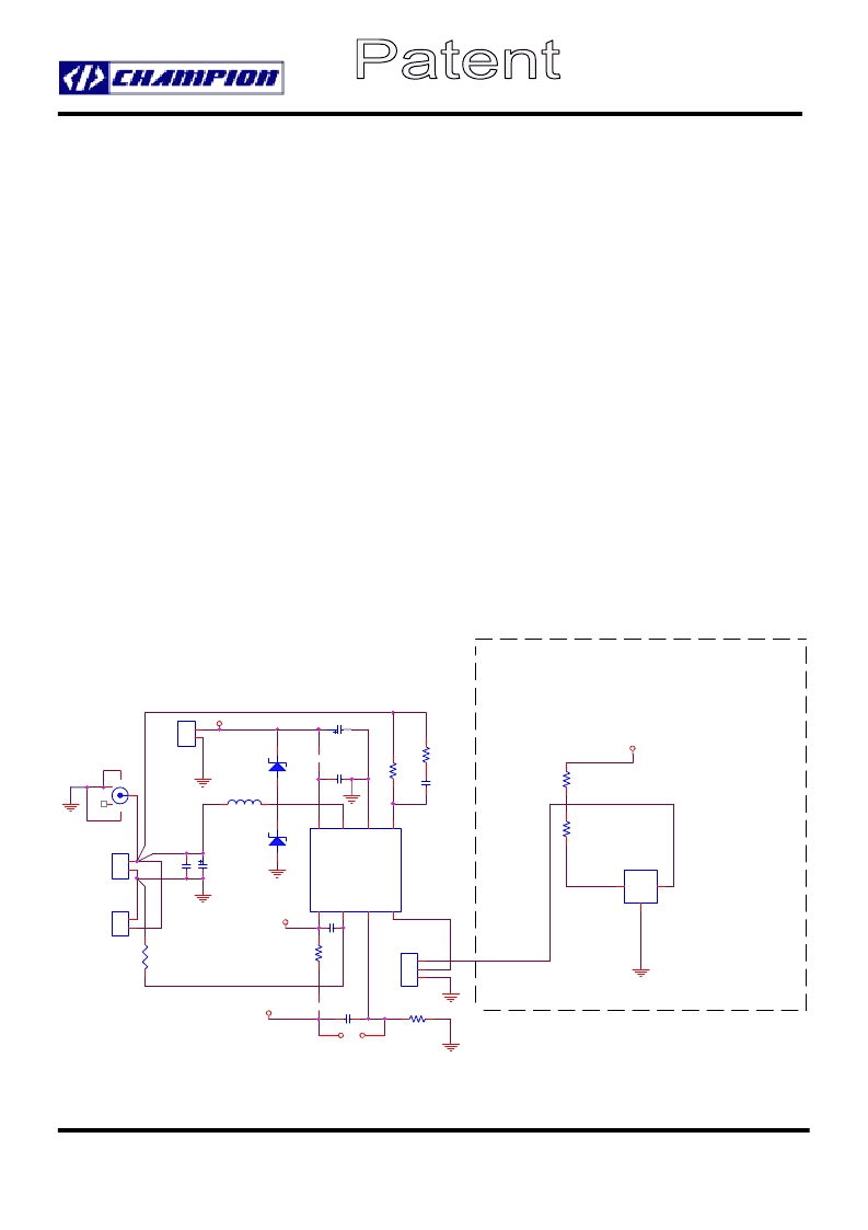
APPLICATION CIRCUIT
INPUTS
The input voltage reference pin, VREF determine the output
voltages (LX). If a specific voltage is forced at the VREF pin, the
output voltage follows the voltage at the VREF pin.
OTHER SUPPLY VOLTAGES
Several inputs are provided for the supply voltages: PVIN and
VIN.
The PVIN provide the power supply to the power MOSFETs.
VIN provides the voltage supply to the logic section and internal
error amplifiers.
FEEDBACK
The VFB pin is an input that can be used for closed loop
compensation. This input is derived from the voltage output.
AGND pin is a contact node of internal resistor divider for
remote sense.
TP1
BNC
1
2
3
4
5
VCC
R4
470
2
1
1
L1
3.3uH/2A
C2
105
R5
0
R3
100k
2
1
U3
CM3718-8PIN
2
1
3
4
5
6
7
8
G
V
S
V
V
P
L
P
VDD
JP1
JUMPER
C3
470
D1
SK12
VCC
JP2
JUMPER
J3
VREF-OUT
1
2
R7
0
2
JP3---->USEING EXTERNAL
VOLTAGE SETING BOARD
(PIN 1,2 SHORT)
C4
105
VDD
J2
VTT
1
2
NOTE:
J1
PWR/IN
1
2
R1
100k
2
1
C7
104
C6
47uf/6.3V
C5
104P
JP3
CON3
3
2
1
JP4
on/off sw
U2 CM-431
1
3
2
R2
1k
2
1
C1
100uf/6.3V
D2
SK12
R8
5.1
2
1
相關(guān)PDF資料 |
PDF描述 |
|---|---|
| CM3728 | 2.5G/3G Cellular Phone Buck Regulator|Battery Management ICs |
| CM4-282B | Optoelectronic |
| CM4-383B | Optoelectronic |
| CM4-384B | Optoelectronic |
| CM4-482B | Optoelectronic |
相關(guān)代理商/技術(shù)參數(shù) |
參數(shù)描述 |
|---|---|
| CM3718GIS | 制造商:未知廠家 制造商全稱:未知廠家 功能描述:1.5A LOW NOISE PWM STEP DOWN REGULATOR |
| CM3718IS | 制造商:CHAMP 制造商全稱:CHAMP 功能描述:1.5A LOW-NOISE PWM STEP-DOWN REGULATOR |
| CM3728 | 制造商:未知廠家 制造商全稱:未知廠家 功能描述:2.5G/3G Cellular Phone Buck Regulator|Battery Management ICs |
| CM373 | 制造商:CML 制造商全稱:Chicago Miniature Lamp,inc 功能描述:T-1 3/4 Wedge Base |
| CM37326 | 制造商:CLAROSTAT 功能描述:POT- 5KOHM |
發(fā)布緊急采購,3分鐘左右您將得到回復(fù)。