- 您現(xiàn)在的位置:買賣IC網 > PDF目錄378881 > CM6824 (Electronic Theatre Controls, Inc.) LOW START-UP CURRENT PFC/PWM CONTROLLER COMBO PDF資料下載
參數(shù)資料
| 型號: | CM6824 |
| 廠商: | Electronic Theatre Controls, Inc. |
| 英文描述: | LOW START-UP CURRENT PFC/PWM CONTROLLER COMBO |
| 中文描述: | 低啟動電流式PFC / PWM控制器組合 |
| 文件頁數(shù): | 4/18頁 |
| 文件大?。?/td> | 342K |
| 代理商: | CM6824 |
CM6824
L
OW
S
TART-
U
P
C
URRENT
PFC/PWM C
ONTROLLER
C
OMBO
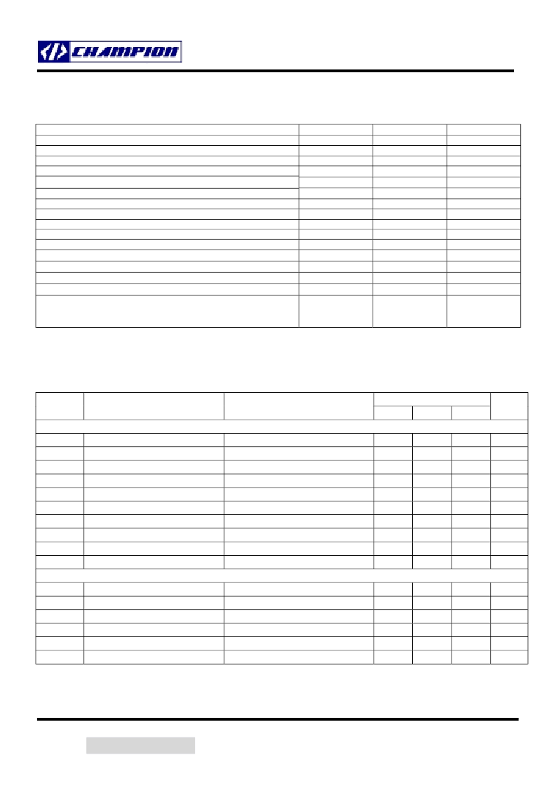
ABSOLUTE MAXIMUM RATINGS
Absolute Maximum ratings are those values beyond which the device could be permanently damaged.
Parameter
V
CC
IEAO
I
SENSE
Voltage
PFC OUT
PWMOUT
Voltage on Any Other Pin
I
REF
I
AC
Input Current
Peak PFC OUT Current, Source or Sink
Peak PWM OUT Current, Source or Sink
PFC OUT, PWM OUT Energy Per Cycle
Junction Temperature
Storage Temperature Range
Operating Temperature Range
Lead Temperature (Soldering, 10 sec)
Thermal Resistance (
θ
JA
)
Plastic DIP
Plastic SOIC
ELECTRICAL CHARACTERISTICS
Unless otherwise stated, these specifications apply Vcc=+15V, R
T
= 52.3k
, C
T
= 470pF, T
A
=Operating Temperature Range (Note 1)
2002/09/20
Preliminary
Rev. 1.1
Champion Microelectronic Corporation
Page 4
Min.
0
-5
GND – 0.3
GND – 0.3
GND – 0.3
-65
-40
Max.
23
4.5
0.7
VCC + 0.3
VCC + 0.3
VREF + 0.3
10
1
1
1
1.5
150
150
125
260
80
105
Units
V
V
V
V
V
V
mA
mA
A
A
μJ
℃
℃
℃
℃
℃
/W
℃
/W
CM6824
Typ.
Symbol
Parameter
Test Conditions
Min.
Max.
Unit
Voltage Error Amplifier (g
mv
)
Input Voltage Range
Transconductance
Feedback Reference Voltage
Input Bias Current
Output High Voltage
Output Low Voltage
Sink Current
Source Current
Open Loop Gain
Power Supply Rejection Ratio
0
50
2.45
-1.0
5.8
30
50
50
5
V
V
NONINV
= V
INV
, VEAO = 3.75V
Note 2
V
FB
= 3V, VEAO = 6V
V
FB
= 1.5V, VEAO = 1.5V
11V < V
CC
< 16.5V
Current Error Amplifier (g
mi
)
85
2.5
-0.5
6.0
0.1
-35
40
60
60
120
2.55
0.4
-20
μmho
V
μA
V
V
μA
μA
dB
dB
Input Voltage Range
Transconductance
Input Offset Voltage
Input Bias Current
Output High Voltage
Output Low Voltage
-1.5
130
-12
-1.0
4.0
0.7
310
12
1.0
V
V
NONINV
= V
INV
, VEAO = 3.75V
195
-0.5
4.25
0.65
μmho
mV
μA
V
V
相關PDF資料 |
PDF描述 |
|---|---|
| CM6824IP | LOW START-UP CURRENT PFC/PWM CONTROLLER COMBO |
| CM6824IS | LOW START-UP CURRENT PFC/PWM CONTROLLER COMBO |
| CM8501GIS | 1.5A BUS TERMINATOR |
| CM8501IS | 1.5A BUS TERMINATOR |
| CM8501IT | 1.5A BUS TERMINATOR |
相關代理商/技術參數(shù) |
參數(shù)描述 |
|---|---|
| CM6824-000 | 制造商:TE Connectivity 功能描述:D-436-37-SNPB - Bulk |
| CM6824IP | 制造商:未知廠家 制造商全稱:未知廠家 功能描述:LOW START-UP CURRENT PFC/PWM CONTROLLER COMBO |
| CM6824IS | 制造商:未知廠家 制造商全稱:未知廠家 功能描述:LOW START-UP CURRENT PFC/PWM CONTROLLER COMBO |
| CM6825-000 | 制造商:TE Connectivity 功能描述:D-436-38-SNPB - Bulk |
| CM683 | 制造商:CML 制造商全稱:Chicago Miniature Lamp,inc 功能描述:T-1 Wire Terminal (standard) |
發(fā)布緊急采購,3分鐘左右您將得到回復。