- 您現(xiàn)在的位置:買賣IC網(wǎng) > PDF目錄295335 > CS3972YDW16 3 A SWITCHING CONTROLLER, 47 kHz SWITCHING FREQ-MAX, PDSO16 PDF資料下載
參數(shù)資料
| 型號: | CS3972YDW16 |
| 元件分類: | 穩(wěn)壓器 |
| 英文描述: | 3 A SWITCHING CONTROLLER, 47 kHz SWITCHING FREQ-MAX, PDSO16 |
| 封裝: | SO-16 |
| 文件頁數(shù): | 4/6頁 |
| 文件大小: | 186K |
| 代理商: | CS3972YDW16 |

The CS3972 has an on board, high current NPN transistor
in its output stage. The output transistor is switched on
every 25s by the on board 40 kHz oscillator. The output
is switched off as soon as the output current reaches a
dynamically controlled level. That level is determined by
three factors: the current drawn by the load, the input
voltage, and the output voltage. This control scheme has
several benefits. The IC reacts quickly to overvoltage and
short circuit conditions and it is less sensitive to input
voltage fluctuation.
Current drawn by the load influences when the output
stage turns off. The voltage across the internal high preci-
sion resistor (0.11) in the emitter of the output transistor
generating the input to the current sensing amplifier. The
output of the current sensing amplifier provides one of the
inputs to the comparator.
The other input to the comparator connected to the out-
put of the error amplifier whose inverting input is con-
nected to the output voltage through the feedback circuit-
ry while its noninverting input is set to an internal refer-
ence voltage of 1.24V. When the current sensing amplifier
output exceeds the error amplifier output, the comparator
switches off, triggering the logic which turns off the out-
put stage.
All on board amplifier, logic and protection circuitry uses
the internal 2.3V reference to minimize quiescent current
drain (6mA) and permits IC operation down to 3V.
The anti-saturation circuitry minimizes output switch
turn off time and power dissipation, by keeping the
power NPN at the edge of saturation.
4
Circuit Description
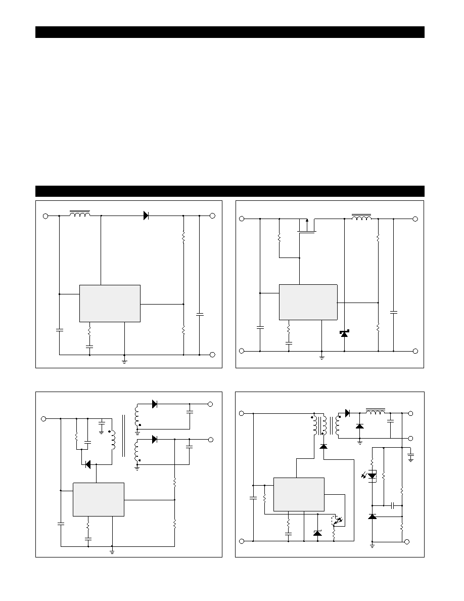
Application Diagrams
VIN
D1
C1
+
R1
C2
R3
C3
(1.24V)
R2
VOUT
VIN
VC
Gnd
VFB
VSW
CS3972
L1
+
VIN
Q1
R1
C1
+
R2
C2
D1
R4
C3
(1.24V)
R3
VOUT
VIN
VC
Gnd
VFB
VSW
CS3972
L1
+
VIN
TR1
R1
C2
+
R2
C3
R5
(1.24V)
R4
VOUT1
VIN
VC
Gnd
VFB
VSW
CS3972
C4
C1
C5
+
C6
+
VOUT2
+VIN
TR1
C2
+
R2
C3
R7
R5
VOUT
VIN
VC
Gnd
VFB
VSW
CS3972
C3
+
C5
L1
D2
D1
R4
1/2
OC1
R6
C4
U1
R3
D1
R1
–VIN
D3
1/2
OC1
Figure 1: Boost Regulator
Figure 2: Buck Regulator with the External Switch
Figure 3: Flyback Multiple Output Regulator
Figure 4: Isolated Forward Regulator
CS3972
相關(guān)PDF資料 |
PDF描述 |
|---|---|
| CS5157GD16 | 1.5 A SWITCHING CONTROLLER, 1000 kHz SWITCHING FREQ-MAX, PDSO16 |
| CS5165GDWR16 | 1.5 A SWITCHING CONTROLLER, 1000 kHz SWITCHING FREQ-MAX, PDSO16 |
| CS5332GDW28 | 1.5 A SWITCHING CONTROLLER, 1000 kHz SWITCHING FREQ-MAX, PDSO28 |
| CS600/L2 | 1 CHANNEL LOGIC OUTPUT OPTOCOUPLER |
| CSBLA384KECE-B0 | CERAMIC RESONATOR, 0.384 MHz |
相關(guān)代理商/技術(shù)參數(shù) |
參數(shù)描述 |
|---|---|
| CS3972YDWR16 | 制造商:Rochester Electronics LLC 功能描述:- Bulk |
| CS3972YN8 | 制造商:Rochester Electronics LLC 功能描述:- Bulk |
| CS3972YT5 | 制造商:CHERRY 制造商全稱:CHERRY 功能描述:1.25A High Efficiency Switching Regulator |
| CS3972YTHA5 | 制造商:CHERRY 制造商全稱:CHERRY 功能描述:1.25A High Efficiency Switching Regulator |
| CS3972YTVA5 | 制造商:CHERRY 制造商全稱:CHERRY 功能描述:1.25A High Efficiency Switching Regulator |
發(fā)布緊急采購,3分鐘左右您將得到回復(fù)。