- 您現(xiàn)在的位置:買(mǎi)賣(mài)IC網(wǎng) > PDF目錄352821 > CS51414GD8 SMPS Controller PDF資料下載
參數(shù)資料
| 型號(hào): | CS51414GD8 |
| 英文描述: | SMPS Controller |
| 中文描述: | 開(kāi)關(guān)電源控制器 |
| 文件頁(yè)數(shù): | 15/16頁(yè) |
| 文件大?。?/td> | 489K |
| 代理商: | CS51414GD8 |
第1頁(yè)第2頁(yè)第3頁(yè)第4頁(yè)第5頁(yè)第6頁(yè)第7頁(yè)第8頁(yè)第9頁(yè)第10頁(yè)第11頁(yè)第12頁(yè)第13頁(yè)第14頁(yè)當(dāng)前第15頁(yè)第16頁(yè)
CS51411, CS51412, CS51413, CS51414
http://onsemi.com
8
VF = diode forward voltage.
The anode of the diode can be connected to any DC voltage
other than the regulated output voltage. However, the
maximum voltage on the BOOST pin shall not exceed 40 V.
As shown in Figure 7, the BOOST pin current includes a
constant 7.0 mA pre–driver current and base current
proportional to switch conducting current. A detailed
discussion of this current is conducted in Thermal
Consideration section. A 0.1
F capacitor is usually
adequate for maintaining the Boost pin voltage during the on
time.
Figure 7. The Boost Pin Current Includes 7.0 mA
Pre–Driver Current and Base Current when the
Switch is Turned On. The Beta Decline of the
Power Switch Further Increases the Base
Current at High Switching Current
0
0.5
1.0
1.5
Switching Current (A)
Boost
Pin
Current
(mA)
0
5
10
15
20
25
30
BIAS Pin (CS51412 and CS51414 Only)
The BIAS pin allows a secondary power supply to bias the
control circuitry of the IC. The BIAS pin voltage should be
between 3.3 V and 6.0 V. If the BIAS pin voltage falls below
that range, use a diode to prevent current drain from the
BIAS pin. Powering the IC with a voltage lower than the
regulator’s input voltage reduces the IC power dissipation
and improves energy transfer efficiency.
Shutdown
The internal power switch will not turn on until the VIN
pin rises above the Start Up Voltage. This ensures no
switching until adequate supply voltage is provided to the
IC.
The IC enters a sleep mode when the SHDNB pin is pulled
below Shutdown Threshold Voltage. In the sleep mode, the
power switch keeps open and the supply current reduces to
Shutdown Quiescent Current. This pin has internal pull–up
current. So when this pin is not used, leave the SHDNB pin
open.
Start–Up
During power up, the regulator tends to quickly charge up
the output capacitors to reach voltage regulation. This gives
rise to an excessive in–rush current which can be detrimental
to the inductor, IC and catch diode. In V2 control , the
compensation capacitor provides Soft Start with no need for
extra pin or circuitry. During the power up, the Output
Source Current of the error amplifier charges the
compensation capacitor which forces VC pin and thus output
voltage ramp up gradually. The Soft Start duration can be
calculated by
TSS +
VC
CCOMP
ISOURCE
where:
VC = VC pin steady–state voltage, which is approximately
equal to error amplifier’s reference voltage.
CCOMP = Compensation capacitor connected to the VC pin
ISOURCE = Output Source Current of the error amplifier.
Using a 0.1
F CCOMP, the calculation shows a TSS over
5.0 ms which is adequate to avoid any current stresses.
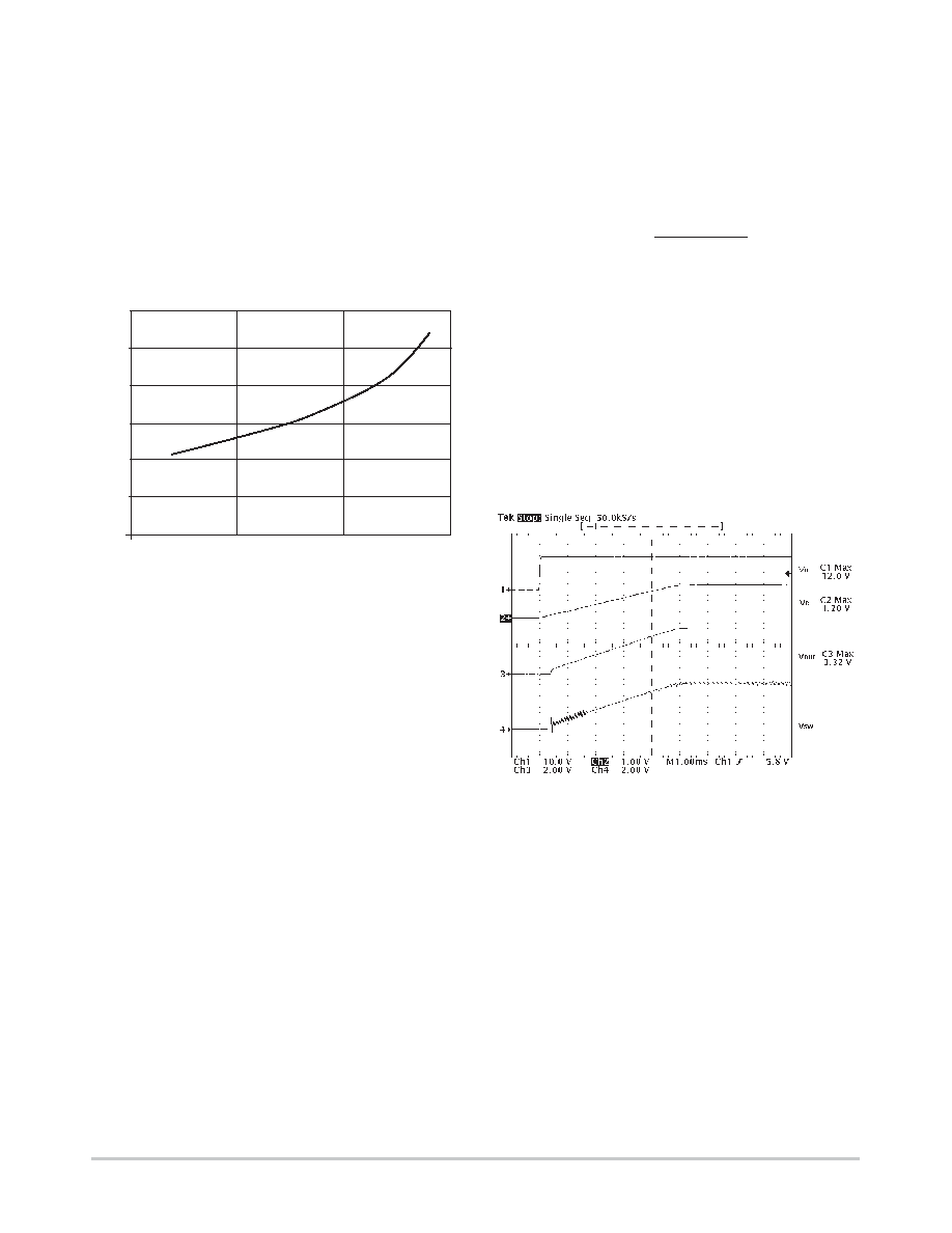
Figure 8 shows the gradual rise of the VC, VO and envelope
of the VSW during power up. There is no voltage over–shoot
after the output voltage reaches the regulation. If the supply
voltage rises slower than the VC pin, output voltage may
over–shoot.
Figure 8. The Power Up Transition of CS5141X
Regulator
Short Circuit
When the VFB pin voltage drops below Foldback
Threshold, the regulator reduces the peak current limit by
40% and switching frequency to 1/4 of the nominal
frequency. These features are designed to protect the IC and
external components during over load or short circuit
conditions. In those conditions, peak switching current is
clamped to the current limit threshold. The reduced
switching frequency significantly increases the ripple
current, and thus lowers the DC current. The short circuit can
cause the minimum duty cycle to be limited by Minimum
Output Pulse Width. The foldback frequency reduces the
minimum duty cycle by extending the switching cycle. This
protects the IC from overheating, and also limits the power
that can be transferred to the output. The current limit
foldback effectively reduces the current stress on the
相關(guān)PDF資料 |
PDF描述 |
|---|---|
| CS51414GDR8 | SMPS Controller |
| CS-514-2DW18 | 2-Channel Disk Read/Write Circuit |
| CS-514-2RDW18 | 2-Channel Disk Read/Write Circuit |
| CS-514-4DW24 | 4-Channel Disk/Tape Read/Write Circuit |
| CS-514-6DW28 | 6-Channel Read/Write Circuit |
相關(guān)代理商/技術(shù)參數(shù) |
參數(shù)描述 |
|---|---|
| CS51414GD8G | 功能描述:直流/直流開(kāi)關(guān)調(diào)節(jié)器 1.5A Low Voltage Buck RoHS:否 制造商:International Rectifier 最大輸入電壓:21 V 開(kāi)關(guān)頻率:1.5 MHz 輸出電壓:0.5 V to 0.86 V 輸出電流:4 A 輸出端數(shù)量: 最大工作溫度: 安裝風(fēng)格:SMD/SMT 封裝 / 箱體:PQFN 4 x 5 |
| CS51414GDR8 | 功能描述:直流/直流開(kāi)關(guān)調(diào)節(jié)器 1.5A Low Voltage RoHS:否 制造商:International Rectifier 最大輸入電壓:21 V 開(kāi)關(guān)頻率:1.5 MHz 輸出電壓:0.5 V to 0.86 V 輸出電流:4 A 輸出端數(shù)量: 最大工作溫度: 安裝風(fēng)格:SMD/SMT 封裝 / 箱體:PQFN 4 x 5 |
| CS51414GDR8G | 功能描述:直流/直流開(kāi)關(guān)調(diào)節(jié)器 1.5A Low Voltage Buck RoHS:否 制造商:International Rectifier 最大輸入電壓:21 V 開(kāi)關(guān)頻率:1.5 MHz 輸出電壓:0.5 V to 0.86 V 輸出電流:4 A 輸出端數(shù)量: 最大工作溫度: 安裝風(fēng)格:SMD/SMT 封裝 / 箱體:PQFN 4 x 5 |
| CS51414GMNR2G | 功能描述:直流/直流開(kāi)關(guān)調(diào)節(jié)器 1.5A 520kHz BUCK REG LOW VOLTAGE RoHS:否 制造商:International Rectifier 最大輸入電壓:21 V 開(kāi)關(guān)頻率:1.5 MHz 輸出電壓:0.5 V to 0.86 V 輸出電流:4 A 輸出端數(shù)量: 最大工作溫度: 安裝風(fēng)格:SMD/SMT 封裝 / 箱體:PQFN 4 x 5 |
| CS5141X-EVM | 制造商:ON Semiconductor 功能描述:CS5141X Evaluation Board |
發(fā)布緊急采購(gòu),3分鐘左右您將得到回復(fù)。