- 您現(xiàn)在的位置:買賣IC網(wǎng) > PDF目錄298969 > CS5205-5GT3 5 V FIXED POSITIVE LDO REGULATOR, 1.3 V DROPOUT, PSFM3 PDF資料下載
參數(shù)資料
| 型號: | CS5205-5GT3 |
| 元件分類: | 固定正電壓單路輸出LDO穩(wěn)壓器 |
| 英文描述: | 5 V FIXED POSITIVE LDO REGULATOR, 1.3 V DROPOUT, PSFM3 |
| 封裝: | STRAIGHT, TO-220, 3 PIN |
| 文件頁數(shù): | 3/7頁 |
| 文件大小: | 160K |
| 代理商: | CS5205-5GT3 |
CS5205-1,-3,-5
3
Package Pin Description
PACKAGE PIN #
PIN SYMBOL
FUNCTION
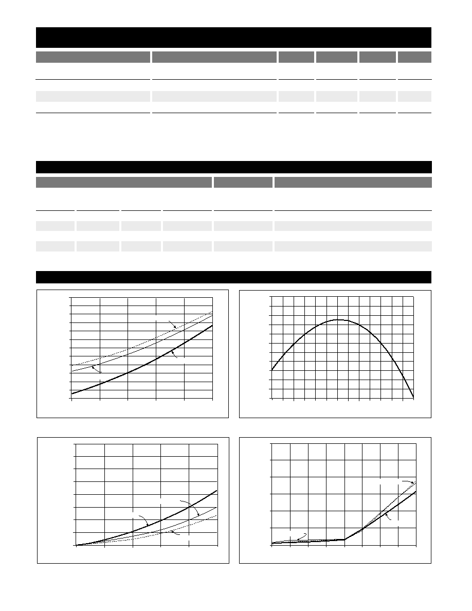
Typical Performance Characteristics
0.85
0.70
0.80
0.90
0.95
1.00
1.05
1.10
1.15
1.20
1.25
1.30
0.75
Dropout
V
oltage
(V)
Output Current (A)
01
2
3
4
5
TCASE = 0°C
TCASE = 125°C
TCASE = 25°C
0
10
130
-0.12
0.10
Output
V
oltage
Deviation
(%)
TJ (°C)
20
30
40
50
60
70
80
90 100 110 120
0.08
0.06
0.04
0.02
0.00
-0.02
-0.04
-0.06
-0.08
-0.10
0.025
0.000
0.050
0.075
0.100
0.200
01
2
3
4
5
Output Current (A)
TCASE = 0°C
0.125
0.150
0.175
TCASE = 125°C
TCASE = 25°C
Output
V
oltage
Deviation
(%)
Dropout Voltage vs. Output Current
Reference Voltage vs. Temperature
Load Regulation vs. Output Current
PARAMETER
TEST CONDITIONS
MIN
TYP
MAX
UNIT
s
Fixed Output Voltage (CS5205-3, -5): continued
RMS Output Noise (%VOUT)
10Hz ≤ f ≤ 10kHz
0.003
%VOUT
Thermal Shutdown
150
180
°C
Thermal Shutdown Hysteresis
25
°C
Note 1: Load regulation and output voltage are measured at a constant junction temperature by low duty cycle pulse testing. Changes in out-
put voltage due to thermal gradients or temperature changes must be taken into account separately.
Note 2: Specifications apply for an external Kelvin sense connection at a point on the output pin 1/4” from the bottom of the package.
Note 3: Dropout voltage is a measurement of the minimum input/output differential at full load.
Electrical Characteristics: CIN = 10F, COUT = 22F Tantalum, VIN – VOUT = 3V, VIN ≤ 10V, 0°C ≤ TA ≤ 70°C, TJ ≤ +150°C,
unless otherwise specified, Ifull load = 5A.
CS5205-1
CS5205-3, -5
D2PAK
3L TO-220
D2PAK
3L TO-220
1
N/A
Adj
Adjust pin (low side of the internal reference).
22
2
VOUT
Regulated output voltage (case).
33
3
VIN
Input voltage.
N/A
1
Gnd
Ground connection.
1
2
3
456
0.550
Minimum
Load
Current
(mA)
VIN – VOUT (V)
TCASE = 0°C
TCASE = 125°C
7
0.875
1.200
1.525
1.850
2.175
2.500
8
9
TCASE = 25°C
Minimum Load Current
相關(guān)PDF資料 |
PDF描述 |
|---|---|
| CS5208-1GT3 | 1.25 V-5 V ADJUSTABLE POSITIVE LDO REGULATOR, 1.3 V DROPOUT, PSFM3 |
| CS5411-4 | Optoelectronic |
| CS5411H4H | Optoelectronic |
| CS54123CP | 高速漏電保護(hù)開關(guān)電路 =M54123L |
| CS5412-AC1 | Analog-to-Digital Converter??? 12-Bit |
相關(guān)代理商/技術(shù)參數(shù) |
參數(shù)描述 |
|---|---|
| CS-5205-5T3 | 制造商:未知廠家 制造商全稱:未知廠家 功能描述:Positive Fixed Voltage Regulator |
| CS5205A-1 | 制造商:CHERRY 制造商全稱:CHERRY 功能描述:5A Adjustable Linear Regulator |
| CS5205A-1/D | 制造商:未知廠家 制造商全稱:未知廠家 功能描述:5A Adjustable Linear Regulator |
| CS-5205A-1DP3 | 制造商:未知廠家 制造商全稱:未知廠家 功能描述:Positive Adjustable Voltage Regulator |
| CS5205A-1GDP3 | 制造商:Rochester Electronics LLC 功能描述:- Bulk |
發(fā)布緊急采購,3分鐘左右您將得到回復(fù)。