- 您現(xiàn)在的位置:買賣IC網(wǎng) > PDF目錄374172 > CS8361YN16 (ZF Electronics Corporation) RGBS VIDEO CABLE MM 10 FT PDF資料下載
參數(shù)資料
| 型號: | CS8361YN16 |
| 廠商: | ZF Electronics Corporation |
| 英文描述: | RGBS VIDEO CABLE MM 10 FT |
| 中文描述: | 5V的雙微功率低壓差穩(wěn)壓器具有使能和重置 |
| 文件頁數(shù): | 4/6頁 |
| 文件大?。?/td> | 169K |
| 代理商: | CS8361YN16 |
4
C
Circuit Description
Application Notes
The
V
TRK
on and off. When the
1.4V(typ), V
TRK
turns off. This input has several hundred
millivolts of hysteresis to prevent spurious output activity
during power-up or power-down.
function switches the output transistor for
ENABLE
lead voltage exceeds
The
trolled by a low voltage detection circuit sensing the V
STBY
(5V) output voltage. This circuit guarantees the
output stays below 1V (0.1V typ) when V
STBY
is as low as
1V to ensure reliable operation of microprocessor-based
systems.
is an open collector NPN transistor, con-
This output uses the same type of output device as V
STBY
,
but is rated for 250mA. The output is configured as a
tracking regulator of the standby output. By using the
standby output as a voltage reference, giving the user an
external programming lead (Adj lead), output voltages
from 5V to 20V are easily realized. The programming is
done with a simple resistor divider (Figure 2), and follow-
ing the formula:
V
TRK
= V
STBY
′
(1 + R1/R2) + I
Adj
′
R1
If another 5V output is needed, simply connect the Adj
lead to the V
TRK
output lead.
V
TRK
Output Voltage
RESET
RESET
RESET Function
ENABLE
ENABLE Function
Output capacitors for the CS8361 are required for stability.
Without them, the regulator outputs will oscillate. Actual
size and type may vary depending upon the application
load and temperature range. Capacitor effective series
resistance (ESR) is also a factor in the IC stability. Worst-
case is determined at the minimum ambient temperature
and maximum load expected.
Output capacitors can be increased in size to any desired
value above the minimum. One possible purpose of this
would be to maintain the output voltages during brief
conditions of negative input transients that might be char-
acteristic of a particular system.
Capacitors must also be rated at all ambient temperatures
expected in the system. To maintain regulator stability
down to -40C, capacitors rated at that temperature must
be used.
More information on capacitor selection for Smart
Regulatorsa is available in the Smart Regulator applica-
tion note, òCompensation for Linear Regulators.ó
The maximum power dissipation for a dual output regula-
tor (Figure 1) is:
PD(max) = {V
IN
(max)DV
OUT1
(min)}I
OUT1
(max)+
{V
IN
(max)DV
OUT2
(min)}I
OUT2
(max)+V
IN
(max)IQ
(1)
Where
V
IN
(max) is the maximum input voltage,
V
OUT1
(min) is the minimum output voltage from V
OUT1
,
V
OUT2
(min) is the minimum output voltage from V
OUT2
,
I
OUT1
(max) is the maximum output current, for the
application
I
OUT2
(max) is the maximum output current, for the
application
I
Q
is the quiescent current the regulator consumes at
I
OUT
(max).
Once the value of PD(max) is known, the maximum per-
missible value of R
Q
JA
can be calculated:
150C - T
A
R
Q
JA
=
(2)
The value of R
Q
JA
can then be compared with those in
the package section of the data sheet. Those packages
with R
Q
JA
's less than the calculated value in equation 2
will keep the die temperature below 150C.
In some cases, none of the packages will be sufficient to
dissipate the heat generated by the IC, and an external
heat sink will be required.
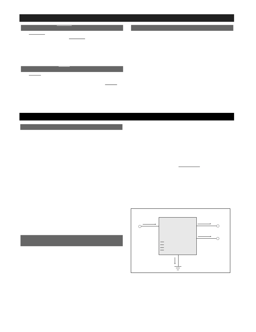
Figure 1: Dual output regulator with key performance parameters
labeled.
V
IN
V
OUT
2
I
IN
I
Q
Control
Features
}
I
OUT
2
V
OUT
1
I
OUT
1
Smart
Regulator
P
D
Calculating Power Dissipation
in a Dual Output Linear Regulator
External Capacitors
相關(guān)PDF資料 |
PDF描述 |
|---|---|
| CS8361YDWF16 | Cap-Free, NMOS, 150mA Low Dropout Regulator with Reverse Current Protection |
| CS8361YDWFR16 | Cap-Free, NMOS, 150mA Low Dropout Regulator with Reverse Current Protection |
| CS8361YDWR20 | Cap-Free, NMOS, 150mA Low Dropout Regulator with Reverse Current Protection |
| CS8361YT7 | Cap-Free, NMOS, 150mA Low Dropout Regulator with Reverse Current Protection |
| CS8371 | 8V/1A, 5V/250mA Dual Regulator with Independent Output Enables and NoCap |
相關(guān)代理商/技術(shù)參數(shù) |
參數(shù)描述 |
|---|---|
| CS8361YT7 | 制造商:CHERRY 制造商全稱:CHERRY 功能描述:5V Dual Micropower Low Dropout Regulator with ENABLE and RESET |
| CS8363 | 制造商:ONSEMI 制造商全稱:ON Semiconductor 功能描述:AC-DC Offline Switching Controllers/Regulators |
| CS8363/D | 制造商:未知廠家 制造商全稱:未知廠家 功能描述:3.3V Dual Micropower Low DropoutRegulator with ENABLEbar and RESETbar |
| CS8363_05 | 制造商:ONSEMI 制造商全稱:ON Semiconductor 功能描述:3.3 V Dual Micropower Low Dropout Regulator with ENABLE and RESET |
| CS8363_11 | 制造商:ONSEMI 制造商全稱:ON Semiconductor 功能描述:3.3 V Dual Micropower Regulator with ENABLE and RESET |
發(fā)布緊急采購,3分鐘左右您將得到回復(fù)。