- 您現在的位置:買賣IC網 > PDF目錄378481 > CY25100SXC-XXXW (CYPRESS SEMICONDUCTOR CORP) Field- and Factory-Programmable Spread Spectrum Clock Generator for EMI Reduction PDF資料下載
參數資料
| 型號: | CY25100SXC-XXXW |
| 廠商: | CYPRESS SEMICONDUCTOR CORP |
| 元件分類: | XO, clock |
| 英文描述: | Field- and Factory-Programmable Spread Spectrum Clock Generator for EMI Reduction |
| 中文描述: | 200 MHz, OTHER CLOCK GENERATOR, PDSO8 |
| 封裝: | 0.150 INCH, LEAD FREE, MS-012, SOIC-8 |
| 文件頁數: | 5/11頁 |
| 文件大?。?/td> | 279K |
| 代理商: | CY25100SXC-XXXW |
CY25100
Document #: 38-07499 Rev. *D
Page 5 of 11
AC Electrical Characteristics
[1]
Parameter
DC
Description
Condition
Min.
45
40
Typ.
50
50
Max.
55
60
Unit
%
%
Output Duty Cycle
Output Duty Cycle
SSCLK, Measured at V
DD
/2
REFCLK, Measured at V
DD
/2
Duty Cycle of CLKIN = 50% at input bias
SSCLK from 3 to 100 MHz; REFCLK from 3 to 100
MHz. 20%–80% of V
DD
SSCLK from 3 to 100 MHz; REFCLK from 3 to 100
MHz. 80%–20% of V
DD
SSCLK from 100 to 200 MHz; REFCLK from 100 to
166 MHz 20%–80% of V
DD
SSCLK from 100 to 200 MHz; REFCLK from 100 to
166 MHz 80%–20% of V
DD
CLKIN = SSCLK = 166 MHz, 2% spread, REFCLK off
CLKIN = SSCLK = 66 MHz, 2% spread, REFCLK off
CLKIN = SSCLK = 33 MHz, 2% spread, REFCLK off
CLKIN = SSCLK = 166 MHz, 2% spread, REFCLK on
CLKIN = SSCLK = 66 MHz, 2% spread, REFCLK on
CLKIN = SSCLK = 33 MHz, 2% spread, REFCLK on
CLKIN = SSCLK = 166 MHz, 2% spread, REFCLK on
CLKIN = SSCLK = 66 MHz, 2% spread REFCLK on
CLKIN = SSCLK = 33 MHz, 2% spread, REFCLK on
Time from falling edge on PD# to stopped outputs
(Asynchronous)
Time from falling edge on OE to stopped outputs
(Asynchronous)
Time from rising edge on OE to outputs at a valid fre-
quency (Asynchronous)
Time from rising edge on PD# to outputs at valid fre-
quency (Asynchronous)
Time from rising edge on PD# to outputs at valid fre-
quency (Asynchronous), reference clock at correct
frequency
SR1
Rising Edge Slew Rate
0.7
1.1
3.6
V/ns
SR2
Falling Edge Slew Rate
0.7
1.1
3.6
V/ns
SR3
Rising Edge Slew Rate
1.2
1.6
4.0
V/ns
SR4
Falling Edge Slew Rate
1.2
1.6
4.0
V/ns
T
CCJ1[2]
Cycle-to-Cycle Jitter
SSCLK (Pin 7)
–
–
–
–
–
–
–
–
–
–
90
100
130
100
105
200
80
100
135
150
120
130
170
130
140
260
100
130
180
350
ps
ps
ps
ps
ps
ps
ps
ps
ps
ns
T
CCJ2[2]
Cycle-to-Cycle Jitter
SSCLK (Pin 7)
T
CCJ3[2]
Cycle-to-Cycle Jitter
REFCLK (Pin 6)
t
STP
Power-down Time
(pin 4 = PD#)
Output Disable Time
(pin 4 = OE)
Output Enable Time
(pin 4 = OE)
Power-up Time,
Crystal is used
Power-up Time,
Reference clock is used
T
OE1
–
150
350
ns
T
OE2
–
150
350
ns
t
PU1
–
3.5
5
ms
t
PU2
–
2
3
ms
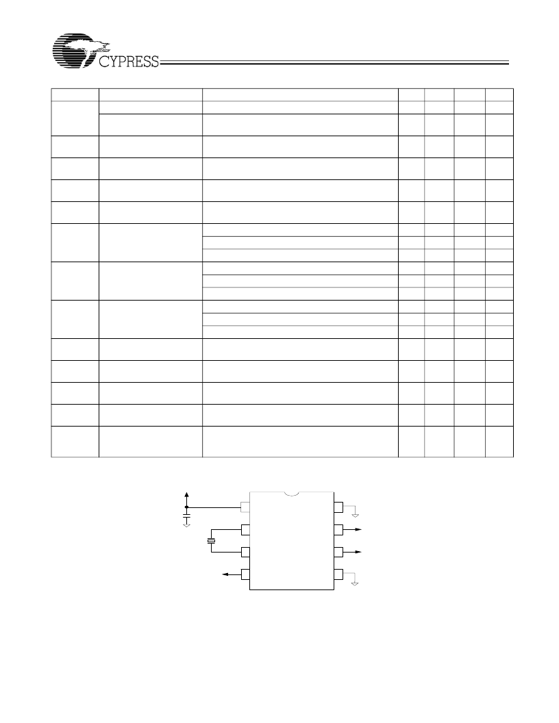
Application Circuit
[3, 4, 5]
2. Jitter is configuration dependent. Actual jitter is dependent on XIN jitter and edge rate, number of active outputs, output frequencies, spread percentage, temper-
ature, and output load. For more information, refer to the application note, “Jitter in PLL Based Systems: Causes, Effects, and Solutions” available at
http://www.cypress.com/clock/appnotes.html, or contact your local Cypress Field Application Engineer.
3. Since the load capacitors (C
and C
) are provided by the CY25100, no external capacitors are needed on the XIN
and XOUT pins to match the crystal load
capacitor (C
). Only a single 0.1-
μ
F bypass capacitor is required on the V
pin.
4. If an external clock is used, apply the clock to XIN (pin 3) and leave XOUT (pin 2) floating (unconnected).
5. If SSON# (pin 8) is LOW (V
SS
), the frequency modulation will be on at SSCLK pin (pin 7).
0 .1 u F
V D D
1
3
2
4
5
6
7
8
V D D
X O U T
X IN /C L K IN
P D # /O E
V S S
R E F C L K
S S C L K
S S O N #
P o w e r
C Y 2 5 1 0 0
相關PDF資料 |
PDF描述 |
|---|---|
| CY25100SXC-XXXWT | Field- and Factory-Programmable Spread Spectrum Clock Generator for EMI Reduction |
| CY25100SXCF | Field- and Factory-Programmable Spread Spectrum Clock Generator for EMI Reduction |
| CY25100SXI-XXXWT | Field- and Factory-Programmable Spread Spectrum Clock Generator for EMI Reduction |
| CY25100ZCF | Field- and Factory-Programmable Spread Spectrum Clock Generator for EMI Reduction |
| CY25100ZXC-XXXW | Field- and Factory-Programmable Spread Spectrum Clock Generator for EMI Reduction |
相關代理商/技術參數 |
參數描述 |
|---|---|
| CY25100SXC-XXXWT | 制造商:CYPRESS 制造商全稱:Cypress Semiconductor 功能描述:Field- and Factory-Programmable Spread Spectrum Clock Generator for EMI Reduction |
| CY25100SXI-030 | 制造商:Rochester Electronics LLC 功能描述: 制造商:Cypress Semiconductor 功能描述: |
| CY25100SXI-030T | 功能描述:時鐘發(fā)生器及支持產品 Spectrum Clk Genratr IND RoHS:否 制造商:Silicon Labs 類型:Clock Generators 最大輸入頻率:14.318 MHz 最大輸出頻率:166 MHz 輸出端數量:16 占空比 - 最大:55 % 工作電源電壓:3.3 V 工作電源電流:1 mA 最大工作溫度:+ 85 C 安裝風格:SMD/SMT 封裝 / 箱體:QFN-56 |
| CY25100SXI-050 | 功能描述:時鐘發(fā)生器及支持產品 Spread Spectrum Clk Gen EMI reduction RoHS:否 制造商:Silicon Labs 類型:Clock Generators 最大輸入頻率:14.318 MHz 最大輸出頻率:166 MHz 輸出端數量:16 占空比 - 最大:55 % 工作電源電壓:3.3 V 工作電源電流:1 mA 最大工作溫度:+ 85 C 安裝風格:SMD/SMT 封裝 / 箱體:QFN-56 |
| CY25100SXI-050T | 功能描述:時鐘發(fā)生器及支持產品 Spread Spectrum Clk Gen EMI reduction RoHS:否 制造商:Silicon Labs 類型:Clock Generators 最大輸入頻率:14.318 MHz 最大輸出頻率:166 MHz 輸出端數量:16 占空比 - 最大:55 % 工作電源電壓:3.3 V 工作電源電流:1 mA 最大工作溫度:+ 85 C 安裝風格:SMD/SMT 封裝 / 箱體:QFN-56 |
發(fā)布緊急采購,3分鐘左右您將得到回復。