- 您現(xiàn)在的位置:買賣IC網(wǎng) > PDF目錄379003 > CY25812ZCT (CYPRESS SEMICONDUCTOR CORP) Spread Spectrum Clock Generator PDF資料下載
參數(shù)資料
| 型號: | CY25812ZCT |
| 廠商: | CYPRESS SEMICONDUCTOR CORP |
| 元件分類: | XO, clock |
| 英文描述: | Spread Spectrum Clock Generator |
| 中文描述: | 64 MHz, OTHER CLOCK GENERATOR, PDSO8 |
| 封裝: | 4.40 MM, TSSOP-8 |
| 文件頁數(shù): | 3/11頁 |
| 文件大?。?/td> | 316K |
| 代理商: | CY25812ZCT |
CY25811/12/14
Document #: 38-07112 Rev. *E
Page 3 of 11
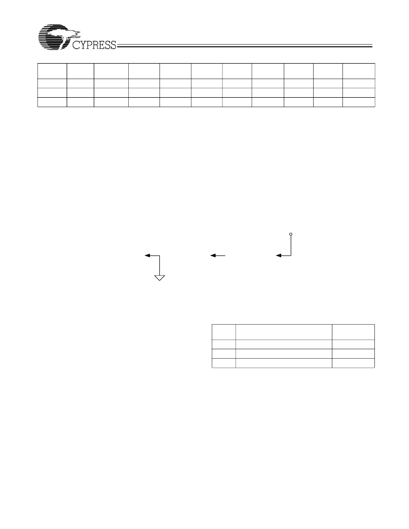
3-Level Digital Inputs
S0, S1, and FRSEL digital inputs are designed to sense 3
different logic levels designated as High “1”, Low “0” and
Middle “M”. With this 3-Level digital input logic, the 3-Level
Logic is able to detect 9 different logic states.
S0, S1 and FRSEL pins include an on chip 20K (10K/10K)
resistor divider. No external application resistors are needed
to implement the 3-Level logic levels as shown below:
Logic Level “0”: 3–Level logic pin connected to GND.
Logic Level “M”: 3–Level logic pin left floating (no connection).
Logic Level “1”: 3–Level logic pin connected to V
DD
.
Figure 1
illustrates how to implement 3–Level Logic.
Modulation Rate
Spread Spectrum Clock Generators utilize frequency
modulation (FM) to distribute energy over a specific band of
frequencies. The maximum frequency of the clock (fmax) and
minimum frequency of the clock (fmin) determine this band of
frequencies. The time required to transition from fmin to fmax
and back to fmin is the period of the Modulation Rate. The
Modulation Rate of SSCG clocks are generally referred to in
terms of frequency, or
fmod = 1/Tmod.
The input clock frequency, fin, and the internal divider
determine the Modulation Rate.
In the case of CY25811/2/4 devices, the (Spread Spectrum)
modulation Rate, fmod, is given by the following formula:
fmod = fin/DR
where; fmod is the Modulation Rate, fin is the Input Frequency
and DR is the Divider Ratio as given in
Table 3
. Notice that
Input Frequency Range is set by FRSEL.
Input and Output Frequency Selection
The relationship between input frequency versus output
frequency in terms of device selection and FRSEL setting is
given in
Table 4
. As shown, the input frequency range is
selected by FRSEL and is the same for CY25811, CY25812,
and CY25814. The selection of CY25811 (1x), CY25812 (2x)
or CY25814 (4x) determines the frequency multiplication at
the output (SSCLK, Pin 5) with respect to input frequency
(XIN, Pin-1).
20-24
24-28
28-32
M
M
M
±1.3
±1.2
±1.1
±1.1
± 0.9
± 0.9
± 0.5
± 0.5
± 0.4
± 0.4
± 0.4
± 0.3
–2.7
–2.5
–2.3
–1.9
–1.8
–1.7
–1.7
–1.5
–1.4
–0.6
–0.6
–0.5
0
0
0
Table 2. Spread% Selection
(continued)
XIN
(MHz)
FRSEL
S1 = 0
S0 = 0
S1 = 0
S0 = M
S1 = 0
S0 = 1
S1 = M
S0 = 0
S1 = 1
S0 = 1
S1 = 1
S0 = 0
S1 = M
S0 = 1
S1 = 1
S0 = M
S1 = M
S0 = M
LOGIC
MIDDLE (M)
LOGIC
HIGH (H)
S0, S1
and
FRSEL
to VDD
S0, S1
and
FRSEL
UNCONNECTED
S0, S1
and
FRSEL
to VSS
VSS
LOGIC
LOW (0)
Figure 1. 3–Level Logic
Table 3. Modulation Rate Divider Ratios
FRSEL
0
1
M
Input Frequency Range
(MHz)
4 to 8
8 to 16
16 to 32
Divider Ratio
(DR)
128
256
512
相關(guān)PDF資料 |
PDF描述 |
|---|---|
| CY25814ZXCT | Spread Spectrum Clock Generator |
| CY25812SIT | Spread Spectrum Clock Generator |
| CY25812ZC | Spread Spectrum Clock Generator |
| CY25812ZXC | Spread Spectrum Clock Generator |
| CY25812ZXCT | Spread Spectrum Clock Generator |
相關(guān)代理商/技術(shù)參數(shù) |
參數(shù)描述 |
|---|---|
| CY25812ZXC | 功能描述:鎖相環(huán) - PLL Reduction SSCGs COM RoHS:否 制造商:Silicon Labs 類型:PLL Clock Multiplier 電路數(shù)量:1 最大輸入頻率:710 MHz 最小輸入頻率:0.002 MHz 輸出頻率范圍:0.002 MHz to 808 MHz 電源電壓-最大:3.63 V 電源電壓-最小:1.71 V 最大工作溫度:+ 85 C 最小工作溫度:- 40 C 封裝 / 箱體:QFN-36 封裝:Tray |
| CY25812ZXCT | 功能描述:鎖相環(huán) - PLL Reduction SSCGs COM RoHS:否 制造商:Silicon Labs 類型:PLL Clock Multiplier 電路數(shù)量:1 最大輸入頻率:710 MHz 最小輸入頻率:0.002 MHz 輸出頻率范圍:0.002 MHz to 808 MHz 電源電壓-最大:3.63 V 電源電壓-最小:1.71 V 最大工作溫度:+ 85 C 最小工作溫度:- 40 C 封裝 / 箱體:QFN-36 封裝:Tray |
| CY25814 | 制造商:未知廠家 制造商全稱:未知廠家 功能描述:Clocks and Buffers |
| CY25814SC | 制造商:CYPRESS 制造商全稱:Cypress Semiconductor 功能描述:Spread Spectrum Clock Generator |
| CY25814SCT | 制造商:Cypress Semiconductor 功能描述: |
發(fā)布緊急采購,3分鐘左右您將得到回復(fù)。