- 您現(xiàn)在的位置:買賣IC網(wǎng) > PDF目錄379003 > CY25814ZC (CYPRESS SEMICONDUCTOR CORP) DB37 INTERFACE DATA CBL DB37 Female - DB37 Female PDF資料下載
參數(shù)資料
| 型號(hào): | CY25814ZC |
| 廠商: | CYPRESS SEMICONDUCTOR CORP |
| 元件分類: | XO, clock |
| 英文描述: | DB37 INTERFACE DATA CBL DB37 Female - DB37 Female |
| 中文描述: | 128 MHz, OTHER CLOCK GENERATOR, PDSO8 |
| 封裝: | 4.40 MM, TSSOP-8 |
| 文件頁(yè)數(shù): | 4/11頁(yè) |
| 文件大小: | 316K |
| 代理商: | CY25814ZC |
CY25811/12/14
Document #: 38-07112 Rev. *E
Page 4 of 11
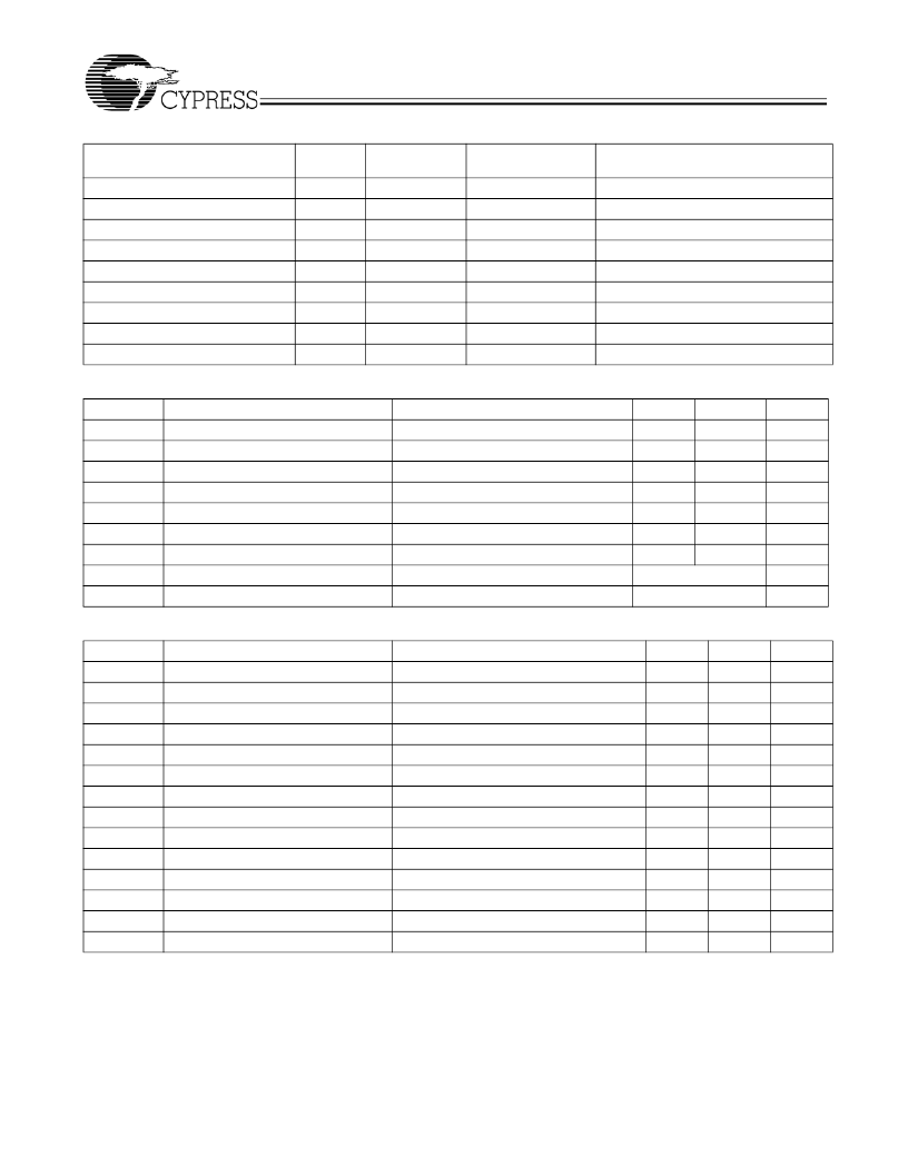
Table 4. Input and Output Frequency Selection
Input Frequency Range
(MHz)
4 to 8
8 to 16
16 to 32
4 to 8
8 to 16
16 to 32
4 to 8
8 to 16
16 to 32
FRSEL
0
1
M
0
1
M
0
1
M
Product
CY25811
CY25811
CY25811
CY25812
CY25812
CY25812
CY25814
CY25814
CY25814
Multiplication
1x
1x
1x
2x
2x
2x
4x
4x
4x
Output Frequency Range
(MHz)
4 to 8
8 to 16
16 to 32
8 to 16
16 to 32
32 to 64
16 to 32
32 to 64
64 to 128
Absolute Maximum Conditions
(both Commercial and Industrial Grades)
[1,2]
Parameter
V
DD
V
IN
T
S
T
A1
T
A2
T
J
ESD
HBM
UL-94
MSL
Description
Condition
Min.
–0.5
–0.5
–65
0
–40
–
2000
Max.
4.6
V
DD
+ 0.5
150
70
85
150
–
V–0
1
Unit
V
VDC
°C
°C
°C
°C
V
Supply Voltage
Input Voltage
Temperature, Storage
Temperature, Operating Ambient
Temperature, Operating Ambient
Temperature, Junction
ESD Protection (Human Body Model) MIL-STD-883, Method 3015
Flammability Rating
Moisture Sensitivity Level
Relative to V
SS
Non Functional
Functional, C-Grade
Functional, I-Grade
Functional
@1/8 in.
DC Electrical Specifications
(Commercial Grade)
Parameter
V
DD
V
IL
V
IM
V
IH
V
OL1
V
OL2
V
OH1
V
OH2
C
IN1
C
IN2
C
L
I
DD1
I
DD2
I
DD3
Notes:
1. Operation at any Absolute Maximum Rating is not implied.
2. Single Power Supply: The voltage on any input or I/O pin cannot exceed the power pin during power up.
Description
Condition
Min.
3.135
0
0.40V
DD
0.85V
DD
–
–
2.4
2.0
6.0
3.5
–
–
–
–
Max.
3.465
0.15V
DD
0.60V
DD
V
DD
0.4
1.2
–
–
9.0
6.0
15
25
30
35
Unit
V
V
V
V
V
V
V
V
pF
pF
pF
mA
mA
mA
3.3 Operating Voltage
Input Low Voltage
Input Middle Voltage
Input High Voltage
Output Low Voltage
Output Low Voltage
Output High Voltage
Output High Voltage
Input Pin Capacitance
Input Pin Capacitance
Output Load Capacitor
Dynamic Supply Current
Dynamic Supply Current
Dynamic Supply Current
3.3 ± 5%
S0, S1 and FRSEL Inputs
S0, S1 and FRSEL Inputs
S0, S1 and FRSEL Inputs
I
OL
= 4 ma, SSCLK Output
I
OL
= 10 ma, SSCLK Output
I
OH
= 4 ma, SSCLK Output
I
OH
= 6 ma, SSCLK Output
XIN (Pin 1) and XOUT (Pin 8)
All Digital Inputs
SSCLK Output
Fin = 12 MHz, no load
Fin = 24 MHz, no load
Fin = 32 MHz, no load
相關(guān)PDF資料 |
PDF描述 |
|---|---|
| CY25811SXIT | Spread Spectrum Clock Generator |
| CY25812ZCT | Spread Spectrum Clock Generator |
| CY25814ZXCT | Spread Spectrum Clock Generator |
| CY25812SIT | Spread Spectrum Clock Generator |
| CY25812ZC | Spread Spectrum Clock Generator |
相關(guān)代理商/技術(shù)參數(shù) |
參數(shù)描述 |
|---|---|
| CY25814ZCT | 制造商:Rochester Electronics LLC 功能描述:- Bulk |
| CY25814ZXC | 制造商:CYPRESS 制造商全稱:Cypress Semiconductor 功能描述:Spread Spectrum Clock Generator |
| CY25814ZXCT | 制造商:CYPRESS 制造商全稱:Cypress Semiconductor 功能描述:Spread Spectrum Clock Generator |
| CY25818 | 制造商:CYPRESS 制造商全稱:Cypress Semiconductor 功能描述:SPREAD SPECTRUM CLOCK GENERATOR |
| CY25818_06 | 制造商:CYPRESS 制造商全稱:Cypress Semiconductor 功能描述:Spread Spectrum Clock Generator |
發(fā)布緊急采購(gòu),3分鐘左右您將得到回復(fù)。