- 您現(xiàn)在的位置:買賣IC網(wǎng) > PDF目錄378482 > CY28326OXCT (CYPRESS SEMICONDUCTOR CORP) Single Pole Normally Open: 1-Form-A PDF資料下載
參數(shù)資料
| 型號(hào): | CY28326OXCT |
| 廠商: | CYPRESS SEMICONDUCTOR CORP |
| 元件分類: | XO, clock |
| 英文描述: | Single Pole Normally Open: 1-Form-A |
| 中文描述: | 333.3 MHz, PROC SPECIFIC CLOCK GENERATOR, PDSO48 |
| 封裝: | LEAD FREE, SSOP-48 |
| 文件頁(yè)數(shù): | 4/23頁(yè) |
| 文件大?。?/td> | 288K |
| 代理商: | CY28326OXCT |
第1頁(yè)第2頁(yè)第3頁(yè)當(dāng)前第4頁(yè)第5頁(yè)第6頁(yè)第7頁(yè)第8頁(yè)第9頁(yè)第10頁(yè)第11頁(yè)第12頁(yè)第13頁(yè)第14頁(yè)第15頁(yè)第16頁(yè)第17頁(yè)第18頁(yè)第19頁(yè)第20頁(yè)第21頁(yè)第22頁(yè)第23頁(yè)
CY28326
Document #: 38-07616 Rev. *A
Page 4 of 23
Serial Data Interface
To enhance the flexibility and function of the clock synthesizer,
a two-signal serial interface is provided. Through the Serial
Data Interface, various device functions, such as individual
clock output buffers, can be individually enabled or disabled.
The registers associated with the Serial Data Interface
initializes to their default setting upon power-up, and therefore
use of this interface is optional. The interface can also be
accessed during power down operation.
Data Protocol
The clock driver serial protocol accepts byte write, byte read,
block write and block read operation from any external I
2
C
controller. For block write/read operation, the bytes must be
accessed in sequential order from lowest to highest byte (most
significant bit first) with the ability to stop after any complete
byte has been transferred. For byte write and byte read opera-
tions, the system controller can access individual indexed
bytes. The offset of the indexed byte is encoded in the
command code, as described in
Table 4
. The block write and
block read protocol is outlined in
Table 5
while
Table 6
outlines
the corresponding byte write and byte read protocol.The slave
receiver address is 11010010 (D2h).
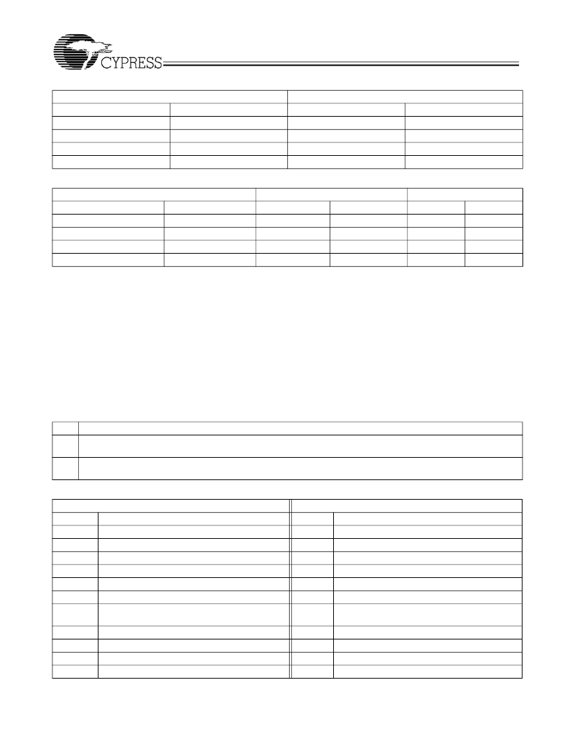
Table 2. Mode Ratio Setting
Power-up Condition
Pin I/O Setting
Mode
0
0
1
1
RatioSel
x
x
0
1
Pin 19
PCI_STP#
PCI_STP#
Ratio0
PCI5
Pin 20
CPU_STP#
CPU_STP#
Ratio1
PCI6
Table 3. Ratio mapping Table
Power-up Frequency value
CPU
100
133
200
166
FS[1:0]
Ratio pin mapping
Pin 20
0
0
1
1
AGP
66.6
66.6
66.6
66.6
FS1
0
0
1
1
FS0
0
1
0
1
Pin 19
0
1
0
1
Table 4. Command Code Definition
Bit
7
Description
0 = Block read or block write operation
1 = Byte read or byte write operation
Device selection bits. Set = 00
Byte offset for byte read or byte write operation. For block read or block write operations, these bits should be '0000000'
(6:5)
(4:0)
Table 5. Block Read and Block Write protocol
Block Write Protocol
Description
Block Read Protocol
Description
Bit
1
8:2
9
10
18:11
19
27:20
Bit
1
8:2
9
10
18:11
19
20
Start
Slave address – 7 bits
Write
Acknowledge from slave
Command Code – 8 Bits
Acknowledge from slave
Byte Count – 8 bits
(Skip this step if I
2
C_EN bit set)
Acknowledge from slave
Data byte 1 – 8 bits
Acknowledge from slave
Data byte 2 – 8 bits
Start
Slave address – 7 bits
Write
Acknowledge from slave
Command Code – 8 Bits
Acknowledge from slave
Repeat start
28
27:21
28
29
37:30
Slave address – 7 bits
Read = 1
Acknowledge from slave
Byte Count from slave – 8 bits
36:29
37
45:38
相關(guān)PDF資料 |
PDF描述 |
|---|---|
| CY28341-2 | Universal Clock Chip for VIA P4M/KT/KM400 DDR Systems |
| CY29962 | 2.5V/3.3V, 150-MHz Multi-Output Zero Delay Buffer |
| CY30 | Sensor interface for an inductive engine wheel speed single rotation sensor |
| CY37128V | 5V, 3.3V, ISR⑩ High-Performance CPLDs |
| CY37256V | 5V, 3.3V, ISR⑩ High-Performance CPLDs |
相關(guān)代理商/技術(shù)參數(shù) |
參數(shù)描述 |
|---|---|
| CY28326SPC | 制造商:Cypress Semiconductor 功能描述: |
| CY28329 | 制造商:SPECTRALINEAR 制造商全稱:SPECTRALINEAR 功能描述:133 MHz Spread Spectrum Clock Synthesizer/Driver with Differential CPU Outputs |
| CY28329OXC | 功能描述:時(shí)鐘驅(qū)動(dòng)器及分配 Intel CK-408B for Plumas chipset RoHS:否 制造商:Micrel 乘法/除法因子:1:4 輸出類型:Differential 最大輸出頻率:4.2 GHz 電源電壓-最大: 電源電壓-最小:5 V 最大工作溫度:+ 85 C 封裝 / 箱體:SOIC-8 封裝:Reel |
| CY28329OXCT | 功能描述:時(shí)鐘驅(qū)動(dòng)器及分配 Intel CK-408B for Plumas chipset RoHS:否 制造商:Micrel 乘法/除法因子:1:4 輸出類型:Differential 最大輸出頻率:4.2 GHz 電源電壓-最大: 電源電壓-最小:5 V 最大工作溫度:+ 85 C 封裝 / 箱體:SOIC-8 封裝:Reel |
| CY28329PVC | 制造商:Cypress Semiconductor 功能描述: |
發(fā)布緊急采購(gòu),3分鐘左右您將得到回復(fù)。