- 您現(xiàn)在的位置:買賣IC網(wǎng) > PDF目錄295374 > CY7C026A Memory PDF資料下載
參數(shù)資料
| 型號(hào): | CY7C026A |
| 英文描述: | Memory |
| 中文描述: | 內(nèi)存 |
| 文件頁數(shù): | 18/20頁 |
| 文件大小: | 301K |
| 代理商: | CY7C026A |

CY7C138AV/144AV/006AV
CY7C139AV/145AV/016AV
CY7C007AV/017AV
Document #: 38-06051 Rev. *A
Page 7 of 20
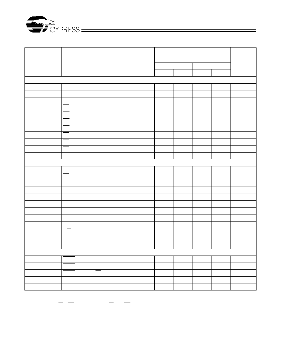
Switching Characteristics Over the Operating Range[15]
Parameter
Description
CY7C138AV/144AV/006AV
CY7C139AV/145AV/016AV
CY7C007AV/017AV
Unit
-20
-25
Min.
Max.
Min.
Max.
READ CYCLE
tRC
Read Cycle Time
20
25
ns
tAA
Address to Data Valid
20
25
ns
tOHA
Output Hold From Address Change
3
ns
tACE
[16]
CE LOW to Data Valid
20
25
ns
tDOE
OE LOW to Data Valid
12
13
ns
tLZOE
[17, 18, 19]
OE Low to Low Z
3
ns
tHZOE
[17, 18, 19]
OE HIGH to High Z
12
15
ns
tLZCE
[17, 18, 19]
CE LOW to Low Z
3
ns
tHZCE
[17, 18, 19]
CE HIGH to High Z
12
15
ns
tPU
[19]
CE LOW to Power-Up
0
ns
tPD
[19]
CE HIGH to Power-Down
20
25
ns
WRITE CYCLE
tWC
Write Cycle Time
20
25
ns
tSCE
[16]
CE LOW to Write End
16
20
ns
tAW
Address Valid to Write End
16
20
ns
tHA
Address Hold From Write End
0
ns
tSA
[16]
Address Set-Up to Write Start
0
ns
tPWE
Write Pulse Width
16
20
ns
tSD
Data Set-Up to Write End
12
15
ns
tHD
Data Hold From Write End
0
ns
tHZWE
[18, 19]
R/W LOW to High Z
12
15
ns
tLZWE
[18, 19]
R/W HIGH to Low Z
3
ns
tWDD
[20]
Write Pulse to Data Delay
40
50
ns
tDDD
[20]
Write Data Valid to Read Data Valid
30
35
ns
BUSY TIMING[21]
tBLA
BUSY LOW from Address Match
20
ns
tBHA
BUSY HIGH from Address Mismatch
20
ns
tBLC
BUSY LOW from CE LOW
20
ns
tBHC
BUSY HIGH from CE HIGH
16
17
ns
tPS
Port Set-Up for Priority
5
ns
Note:
15. Test conditions assume signal transition time of 3 ns or less, timing reference levels of 1.5V, input pulse levels of 0 to 3.0V, and output loading of the specified
IOI/IOH and 30-pF load capacitance.
16. To access RAM, CE=L, SEM=H. To access semaphore, CE=H and SEM=L. Either condition must be valid for the entire tSCE time.
17. At any given temperature and voltage condition for any given device, tHZCE is less than tLZCE and tHZOE is less than tLZOE.
18. Test conditions used are Load 3.
19. This parameter is guaranteed but not tested. For information on port-to-port delay through RAM cells from writing port to reading port, refer to Read Timing
with Busy waveform.
20. For information on port-to-port delay through RAM cells from writing port to reading port, refer to Read Timing with Busy waveform.
21. Test conditions used are Load 2.
相關(guān)PDF資料 |
PDF描述 |
|---|---|
| CY7C026A-12AC | x16 Dual-Port SRAM |
| CY7C026A-15AC | x16 Dual-Port SRAM |
| CY7C026A-15AI | x16 Dual-Port SRAM |
| CY7C026A-20AC | x16 Dual-Port SRAM |
| CY7C026AV | Memory |
相關(guān)代理商/技術(shù)參數(shù) |
參數(shù)描述 |
|---|---|
| CY7C026A_05 | 制造商:CYPRESS 制造商全稱:Cypress Semiconductor 功能描述:16K x 16/18 Dual-Port Static RAM |
| CY7C026A_12 | 制造商:CYPRESS 制造商全稱:Cypress Semiconductor 功能描述:16K x 16 Dual-Port Static RAM |
| CY7C026A-12AC | 制造商:CYPRESS 制造商全稱:Cypress Semiconductor 功能描述:16K x 16/18 Dual-Port Static RAM |
| CY7C026A-15AC | 制造商:Rochester Electronics LLC 功能描述:5V 16K X 16 DPSRAM - Bulk |
| CY7C026A-15AI | 制造商:未知廠家 制造商全稱:未知廠家 功能描述:x16 Dual-Port SRAM |
發(fā)布緊急采購,3分鐘左右您將得到回復(fù)。