- 您現(xiàn)在的位置:買賣IC網(wǎng) > PDF目錄379056 > CY7C1061AV33-12ZXI (CYPRESS SEMICONDUCTOR CORP) 16-Mbit (1M x 16) Static RAM PDF資料下載
參數(shù)資料
| 型號: | CY7C1061AV33-12ZXI |
| 廠商: | CYPRESS SEMICONDUCTOR CORP |
| 元件分類: | DRAM |
| 英文描述: | 16-Mbit (1M x 16) Static RAM |
| 中文描述: | 1M X 16 STANDARD SRAM, 12 ns, PDSO54 |
| 封裝: | LEAD FREE, TSOP2-54 |
| 文件頁數(shù): | 4/10頁 |
| 文件大?。?/td> | 566K |
| 代理商: | CY7C1061AV33-12ZXI |
CY7C1061AV33
Document #: 38-05256 Rev. *G
Page 4 of 10
Notes
6. Test conditions assume signal transition time of 3 ns or less, timing reference levels of 1.5V, input pulse levels of 0 to 3.0V, and output loading of the specified
I
/I
and specified transmission line loads. Test conditions for the Read cycle use output loading shown in (a) of the
“AC Test Loads and Waveforms
” on
page 3
, unless specified otherwise.
7. This part has a voltage regulator that steps down the voltage from 3V to 2V internally. t
time must be provided initially before a Read/Write operation is started.
8. t
, t
, t
, t
HZBE
and t
, t
, t
, t
are specified with a load capacitance of 5 pF as in (b) of
“AC Test Loads and Waveforms
” on page 3
.
Transition is measured
200 mV from steady-state voltage.
9. These parameters are guaranteed by design and are not tested.
10.The internal Write time of the memory is defined by the overlap of CE
LOW (CE
HIGH) and WE LOW. Chip enables must be active and WE and byte enables
must be LOW to initiate a Write, and the transition of any of these signals can terminate the Write. The input data setup and hold timing should be referenced to
the leading edge of the signal that terminates the Write.
11. The minimum Write cycle time for Write Cycle No. 2 (WE controlled, OE LOW) is the sum of t
HZWE
and t
SD
.
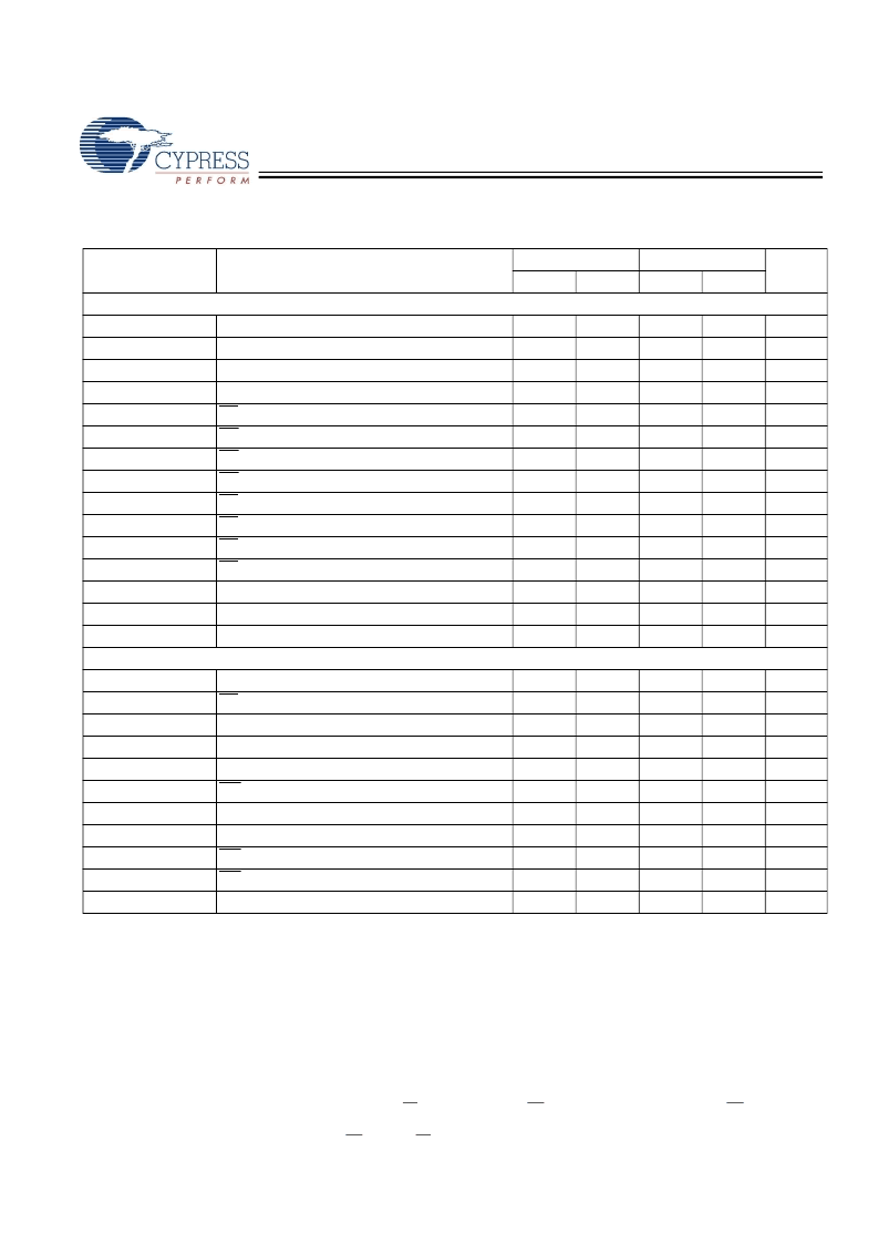
AC Switching Characteristics
(Over the Operating Range)
[6]
Parameter
Description
–10
–12
Unit
Min
Max
Min
Max
Read Cycle
t
power
t
RC
t
AA
t
OHA
t
ACE
t
DOE
t
LZOE
t
HZOE
t
LZCE
t
HZCE
t
PU
t
PD
t
DBE
t
LZBE
t
HZBE
Write Cycle
[10, 11]
V
CC
(typical) to the first access
[7]
Read Cycle Time
1
1
ms
10
12
ns
Address to Data Valid
10
12
ns
Data Hold from Address Change
3
3
ns
CE
1
LOW/CE
2
HIGH to Data Valid
OE LOW to Data Valid
10
12
ns
5
6
ns
OE LOW to Low-Z
OE HIGH to High-Z
[8]
CE
1
LOW/CE
2
HIGH to Low-Z
[8]
CE
1
HIGH/CE
2
LOW to High-Z
[8]
CE
1
LOW/CE
2
HIGH to Power Up
[9]
CE
1
HIGH/CE
2
LOW to Power Down
[9]
Byte Enable to Data Valid
1
1
ns
5
6
ns
3
3
ns
5
6
ns
0
0
ns
10
12
ns
5
6
ns
Byte Enable to Low-Z
1
1
ns
Byte Disable to High-Z
5
6
ns
t
WC
t
SCE
t
AW
t
HA
t
SA
t
PWE
t
SD
t
HD
t
LZWE
t
HZWE
t
BW
Write Cycle Time
10
12
ns
CE
1
LOW/CE
2
HIGH to Write End
Address Setup to Write End
7
8
ns
7
8
ns
Address Hold from Write End
0
0
ns
Address Setup to Write Start
0
0
ns
WE Pulse Width
7
8
ns
Data Setup to Write End
5.5
6
ns
Data Hold from Write End
WE HIGH to Low-Z
[8]
WE LOW to High-Z
[8]
0
0
ns
3
3
ns
5
6
ns
Byte Enable to End of Write
7
8
ns
[+] Feedback
相關(guān)PDF資料 |
PDF描述 |
|---|---|
| CY7C1061BV33 | 16-Mbit (1M x 16) Static RAM |
| CY7C1061BV33-10ZC | 16-Mbit (1M x 16) Static RAM |
| CY7C1061BV33-10ZI | 16-Mbit (1M x 16) Static RAM |
| CY7C1061BV33-10ZXC | 16-Mbit (1M x 16) Static RAM |
| CY7C1061BV33-10ZXI | 16-Mbit (1M x 16) Static RAM |
相關(guān)代理商/技術(shù)參數(shù) |
參數(shù)描述 |
|---|---|
| CY7C1061AV33-12ZXIT | 功能描述:IC SRAM 16MBIT 12NS 54TSOP RoHS:是 類別:集成電路 (IC) >> 存儲器 系列:- 標(biāo)準(zhǔn)包裝:1,000 系列:- 格式 - 存儲器:RAM 存儲器類型:移動 SDRAM 存儲容量:256M(8Mx32) 速度:133MHz 接口:并聯(lián) 電源電壓:1.7 V ~ 1.95 V 工作溫度:-40°C ~ 85°C 封裝/外殼:90-VFBGA 供應(yīng)商設(shè)備封裝:90-VFBGA(8x13) 包裝:帶卷 (TR) 其它名稱:557-1327-2 |
| CY7C1061AV33-15ZC | 制造商:Cypress Semiconductor 功能描述:16MB- (1MX16) FAST ASYNCH SRAM 3.3V TSOP II 54 - Bulk |
| CY7C1061BV33-10ZXC | 制造商:Rochester Electronics LLC 功能描述: 制造商:Cypress Semiconductor 功能描述: |
| CY7C1061BV33-8ZC | 制造商:Cypress Semiconductor 功能描述:SRAM Chip Async Single 3.3V 16M-Bit 1M x 16 8ns 54-Pin TSOP-II 制造商:Cypress Semiconductor 功能描述:SRAM ASYNC SGL 3.3V 16MBIT 1MX16 8NS 54TSOP-II - Bulk 制造商:Rochester Electronics LLC 功能描述:16MB- (1MX16) FAST ASYNCH SRAM 3.3V TSOP II 54 - Bulk |
| CY7C1061BV33-8ZXC | 制造商:Cypress Semiconductor 功能描述:1M x 16 CPG Fast Async SRAM 制造商:Cypress Semiconductor 功能描述:16MB- (1MX16) FAST ASYNCH SRAM 3.3V TSOP II 54 - Bulk |
發(fā)布緊急采購,3分鐘左右您將得到回復(fù)。