- 您現(xiàn)在的位置:買賣IC網(wǎng) > PDF目錄379060 > CY7C1347G-133BGXI (CYPRESS SEMICONDUCTOR CORP) 4-Mbit (128K x 36) Pipelined Sync SRAM PDF資料下載
參數(shù)資料
| 型號: | CY7C1347G-133BGXI |
| 廠商: | CYPRESS SEMICONDUCTOR CORP |
| 元件分類: | DRAM |
| 英文描述: | 4-Mbit (128K x 36) Pipelined Sync SRAM |
| 中文描述: | 128K X 36 CACHE SRAM, 4 ns, PBGA119 |
| 封裝: | 14 X 22 MM, 2.40 MM HEIGHT, LEAD FREE, BGA-119 |
| 文件頁數(shù): | 5/21頁 |
| 文件大小: | 841K |
| 代理商: | CY7C1347G-133BGXI |
CY7C1347G
Document #: 38-05516 Rev. *E
Page 5 of 21
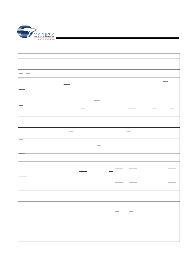
Pin Definitions
Name
IO
Description
A
0
,A
1
,A
Input-
Synchronous
Address Inputs used to select one of the 128K address locations
. Sampled at the rising
edge of the CLK if ADSP or ADSC is active LOW, and CE
1
,
CE
2
, and
CE
3
are sampled active.
A
[1:0]
feeds the 2-bit counter.
Byte Write Select Inputs, Active LOW
. Qualified with BWE to conduct byte writes to the
SRAM. Sampled on the rising edge of CLK.
BW
A,
BW
B,
BW
C,
BW
D
GW
Input-
Synchronous
Input-
Synchronous
Global Write Enable Input, Active LOW
. When asserted LOW on the rising edge of CLK,
a global write is conducted (ALL bytes are written, regardless of the values on BW
[A:D]
and
BWE).
BWE
Input-
Synchronous
Byte Write Enable Input, Active LOW
. Sampled on the rising edge of CLK. This signal must
be asserted LOW to conduct a byte write.
CLK
Input-Clock
Clock Input
. Used to capture all synchronous inputs to the device. Also used to increment
the burst counter when ADV is asserted LOW, during a burst operation.
CE
1
Input-
Synchronous
Chip Enable 1 Input, Active LOW
. Sampled on the rising edge of CLK. Used in conjunction
with CE
2
and CE
3
to select or deselect the device. ADSP is ignored if CE
1
is HIGH. CE
1
is
sampled only when a new external address is loaded.
CE
2
Input-
Synchronous
Chip Enable 2 Input, Active HIGH
. Sampled on the rising edge of CLK. Used in conjunction
with CE
1
and CE
3
to select or deselect the device. CE
2
is sampled only when a new external
address is loaded.
CE
3
Input-
Synchronous
Chip Enable 3 Input, Active LOW
. Sampled on the rising edge of CLK. Used in conjunction
with CE
1
and
CE
2
to select or deselect the device. CE
3
is sampled only when a new external
address is loaded.
OE
Input-
Asynchronous
Output Enable, Asynchronous Input, Active LOW
. Controls the direction of the IO pins.
When LOW, the IO pins behave as outputs. When deasserted HIGH, IO pins are tri-stated,
and act as input data pins. OE is masked during the first clock of a read cycle when emerging
from a deselected state.
ADV
Input-
Synchronous
Advance Input Signal, sampled on the rising edge of CLK
. When asserted, it automati-
cally increments the address in a burst cycle.
ADSP
Input-
Synchronous
Address Strobe from Processor, sampled on the rising edge of CLK
. When asserted
LOW, addresses presented to the device are captured in the address registers. A
[1:0]
are
also loaded into the burst counter. When ADSP and ADSC are both asserted, only ADSP is
recognized. ASDP is ignored when CE
1
is deasserted HIGH.
Address Strobe from Controller, sampled on the rising edge of CLK
. When asserted
LOW, addresses presented to the device are captured in the address registers. A
[1:0]
are
also loaded into the burst counter. When ADSP and ADSC are both asserted, only ADSP is
recognized.
ADSC
Input-
Synchronous
ZZ
Input-
Asynchronous
ZZ “Sleep” Input
. This active HIGH input places the device in a non-time-critical “sleep”
condition with data integrity preserved. During normal operation, this pin must be LOW or
left floating. ZZ pin has an internal pull down.
DQ
A,
DQ
B
DQ
C,
DQ
D
DQP
A,
DQP
B,
DQP
C,
DQP
D
IO-
Synchronous
Bidirectional Data IO Lines
. As inputs, they feed into an on-chip data register that is
triggered by the rising edge of CLK. As outputs, they deliver the data contained in the memory
location specified by the addresses presented during the previous clock rise of the read cycle.
The direction of the pins is controlled by OE. When OE is asserted LOW, the pins behave
as outputs. When HIGH, DQs and DQPs are placed in a tri-state condition.
V
DD
V
SS
V
DDQ
Power Supply
Power supply inputs to the core of the device
.
Ground
Ground for the core of the device
.
IO Power
Supply
Power supply for the IO circuitry
.
V
SSQ
IO Ground
Ground for the IO circuitry
.
[+] Feedback
相關(guān)PDF資料 |
PDF描述 |
|---|---|
| CY7C1347G-133BZC | 4-Mbit (128K x 36) Pipelined Sync SRAM |
| CY7C1347G-133BZI | 4-Mbit (128K x 36) Pipelined Sync SRAM |
| CY7C1347G-133BZXC | 4-Mbit (128K x 36) Pipelined Sync SRAM |
| CY7C1347G-133BZXI | 4-Mbit (128K x 36) Pipelined Sync SRAM |
| CY7C1347G-166AXC | 4-Mbit (128K x 36) Pipelined Sync SRAM |
相關(guān)代理商/技術(shù)參數(shù) |
參數(shù)描述 |
|---|---|
| CY7C1347G-133BGXIT | 功能描述:靜態(tài)隨機存取存儲器 128Kx36 3.3V IND Sync FT 靜態(tài)隨機存取存儲器 RoHS:否 制造商:Cypress Semiconductor 存儲容量:16 Mbit 組織:1 M x 16 訪問時間:55 ns 電源電壓-最大:3.6 V 電源電壓-最小:2.2 V 最大工作電流:22 uA 最大工作溫度:+ 85 C 最小工作溫度:- 40 C 安裝風格:SMD/SMT 封裝 / 箱體:TSOP-48 封裝:Tray |
| CY7C1347G-133BZC | 功能描述:靜態(tài)隨機存取存儲器 128Kx36 3.3V COM Sync FT 靜態(tài)隨機存取存儲器 RoHS:否 制造商:Cypress Semiconductor 存儲容量:16 Mbit 組織:1 M x 16 訪問時間:55 ns 電源電壓-最大:3.6 V 電源電壓-最小:2.2 V 最大工作電流:22 uA 最大工作溫度:+ 85 C 最小工作溫度:- 40 C 安裝風格:SMD/SMT 封裝 / 箱體:TSOP-48 封裝:Tray |
| CY7C1347G-133BZXC | 功能描述:靜態(tài)隨機存取存儲器 128Kx36 3.3V COM Sync FT 靜態(tài)隨機存取存儲器 RoHS:否 制造商:Cypress Semiconductor 存儲容量:16 Mbit 組織:1 M x 16 訪問時間:55 ns 電源電壓-最大:3.6 V 電源電壓-最小:2.2 V 最大工作電流:22 uA 最大工作溫度:+ 85 C 最小工作溫度:- 40 C 安裝風格:SMD/SMT 封裝 / 箱體:TSOP-48 封裝:Tray |
| CY7C1347G-166AXC | 功能描述:靜態(tài)隨機存取存儲器 128Kx36 3.3V COM Sync FT 靜態(tài)隨機存取存儲器 RoHS:否 制造商:Cypress Semiconductor 存儲容量:16 Mbit 組織:1 M x 16 訪問時間:55 ns 電源電壓-最大:3.6 V 電源電壓-最小:2.2 V 最大工作電流:22 uA 最大工作溫度:+ 85 C 最小工作溫度:- 40 C 安裝風格:SMD/SMT 封裝 / 箱體:TSOP-48 封裝:Tray |
| CY7C1347G-166AXCT | 功能描述:靜態(tài)隨機存取存儲器 128Kx36 3.3V COM Sync FT 靜態(tài)隨機存取存儲器 RoHS:否 制造商:Cypress Semiconductor 存儲容量:16 Mbit 組織:1 M x 16 訪問時間:55 ns 電源電壓-最大:3.6 V 電源電壓-最小:2.2 V 最大工作電流:22 uA 最大工作溫度:+ 85 C 最小工作溫度:- 40 C 安裝風格:SMD/SMT 封裝 / 箱體:TSOP-48 封裝:Tray |
發(fā)布緊急采購,3分鐘左右您將得到回復。