- 您現(xiàn)在的位置:買賣IC網(wǎng) > PDF目錄378502 > CY7C1381C-100BZC (CYPRESS SEMICONDUCTOR CORP) 18-Mb (512K x 36/1M x 18) Flow-Through SRAM PDF資料下載
參數(shù)資料
| 型號(hào): | CY7C1381C-100BZC |
| 廠商: | CYPRESS SEMICONDUCTOR CORP |
| 元件分類: | DRAM |
| 英文描述: | 18-Mb (512K x 36/1M x 18) Flow-Through SRAM |
| 中文描述: | 512K X 36 STANDARD SRAM, 8.5 ns, PBGA165 |
| 封裝: | 13 X 15 MM, 1.20 MM HEIGHT, FBGA-165 |
| 文件頁(yè)數(shù): | 13/36頁(yè) |
| 文件大?。?/td> | 564K |
| 代理商: | CY7C1381C-100BZC |
第1頁(yè)第2頁(yè)第3頁(yè)第4頁(yè)第5頁(yè)第6頁(yè)第7頁(yè)第8頁(yè)第9頁(yè)第10頁(yè)第11頁(yè)第12頁(yè)當(dāng)前第13頁(yè)第14頁(yè)第15頁(yè)第16頁(yè)第17頁(yè)第18頁(yè)第19頁(yè)第20頁(yè)第21頁(yè)第22頁(yè)第23頁(yè)第24頁(yè)第25頁(yè)第26頁(yè)第27頁(yè)第28頁(yè)第29頁(yè)第30頁(yè)第31頁(yè)第32頁(yè)第33頁(yè)第34頁(yè)第35頁(yè)第36頁(yè)
CY7C1381C
CY7C1383C
Document #: 38-05238 Rev. *B
Page 13 of 36
Functional Overview
All synchronous inputs pass through input registers controlled
by the rising edge of the clock. Maximum access delay from
the clock rise (t
C0
) is 6.5 ns (133-MHz device).
The CY7C1381C/CY7C1383C supports secondary cache in
systems utilizing either a linear or interleaved burst sequence.
The interleaved burst order supports Pentium
and i486
processors. The linear burst sequence is suited for processors
that utilize a linear burst sequence. The burst order is
user-selectable, and is determined by sampling the MODE
input. Accesses can be initiated with either the Processor
Address Strobe (ADSP) or the Controller Address Strobe
(ADSC). Address advancement through the burst sequence is
controlled by the ADV input. A two-bit on-chip wraparound
burst counter captures the first address in a burst sequence
and automatically increments the address for the rest of the
burst access.
Byte write operations are qualified with the Byte Write Enable
(BWE) and Byte Write Select (BW
X
) inputs. A Global Write
Enable (GW) overrides all byte write inputs and writes data to
all four bytes. All writes are simplified with on-chip
synchronous self-timed write circuitry.
Three synchronous Chip Selects (CE
1
, CE
2
, CE
3[2]
) and an
asynchronous Output Enable (OE) provide for easy bank
selection and output tri-state control. ADSP is ignored if CE
1
is HIGH.
Single Read Accesses
A single read access is initiated when the following conditions
are satisfied at clock rise: (1) CE
1
, CE
2
, and CE
3[2]
are all
asserted active, and (2) ADSP or ADSC is asserted LOW (if
the access is initiated by ADSC, the write inputs must be
deasserted during this first cycle). The address presented to
the address inputs is latched into the address register and the
burst counter/control logic and presented to the memory core.
If the OE input is asserted LOW, the requested data will be
available at the data outputs a maximum to t
CDV
after clock
rise. ADSP is ignored if CE
1
is HIGH.
Single Write Accesses Initiated by ADSP
This access is initiated when the following conditions are
satisfied at clock rise: (1) CE
, CE
, CE
3[2]
are all asserted
active, and (2) ADSP is asserted LOW. The addresses
presented are loaded into the address register and the burst
inputs (GW, BWE, and BW
X
)are ignored during this first clock
cycle. If the write inputs are asserted active ( see Write Cycle
Descriptions table for appropriate states that indicate a write)
on the next clock rise,the appropriate data will be latched and
written into the device.Byte writes are allowed. All I/Os are
tri-stated during a byte write.Since this is a common I/O
device, the asynchronous OE input signal must be deasserted
and the I/Os must be tri-stated prior to the presentation of data
to DQs. As a safety precaution, the data lines are tri-stated
once a write cycle is detected, regardless of the state of OE.
Single Write Accesses Initiated by ADSC
This write access is initiated when the following conditions are
satisfied at clock rise: (1) CE
1
, CE
2
, and CE
3[2]
are all asserted
active, (2) ADSC is asserted LOW, (3) ADSP is deasserted
HIGH, and (4) the write input signals (GW, BWE, and BW
X
)
indicate a write access. ADSC is ignored if ADSP is active LOW.
The addresses presented are loaded into the address register
and the burst counter/control logic and delivered to the
memory core. The information presented to DQ
[A:D]
will be
written into the specified address location. Byte writes are
allowed. All I/Os are tri-stated when a write is detected, even
a byte write. Since this is a common I/O device, the
asynchronous OE input signal must be deasserted and the
I/Os must be tri-stated prior to the presentation of data to DQs.
As a safety precaution, the data lines are tri-stated once a write
cycle is detected, regardless of the state of OE.
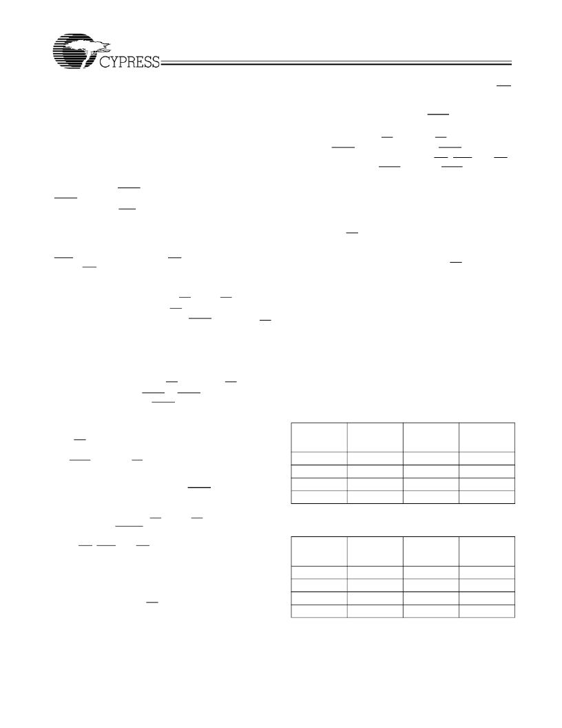
Burst Sequences
The CY7C1381C/CY7C1383C provides an on-chip two-bit
wraparound burst counter inside the SRAM. The burst counter
is fed by A
[1:0]
, and can follow either a linear or interleaved
burst order. The burst order is determined by the state of the
MODE input. A LOW on MODE will select a linear burst
sequence. A HIGH on MODE will select an interleaved burst
order. Leaving MODE unconnected will cause the device to
default to a interleaved burst sequence.
Interleaved Burst Address Table
(MODE = Floating or V
DD
)
First
Address
A1: A0
00
01
10
11
Linear Burst Address Table
(MODE = GND)
Second
Address
A1: A0
01
00
11
10
Third
Address
A1: A0
10
11
00
01
Fourth
Address
A1: A0
11
10
01
00
First
Address
A1: A0
00
01
10
11
Second
Address
A1: A0
01
10
11
00
Third
Address
A1: A0
10
11
00
01
Fourth
Address
A1: A0
11
00
01
10
相關(guān)PDF資料 |
PDF描述 |
|---|---|
| CY7C1383C-133BZC | 18-Mb (512K x 36/1M x 18) Flow-Through SRAM |
| CY7C1381C-100AC | 18-Mb (512K x 36/1M x 18) Flow-Through SRAM |
| CY7C1381C-100AI | 18-Mb (512K x 36/1M x 18) Flow-Through SRAM |
| CY7C1383C-133AC | CAP .22UF 50V POLY B SERIES |
| CY7C1383C-133BGC | 18-Mb (512K x 36/1M x 18) Flow-Through SRAM |
相關(guān)代理商/技術(shù)參數(shù) |
參數(shù)描述 |
|---|---|
| CY7C1381C-100BZI | 制造商:Cypress Semiconductor 功能描述: 制造商:Rochester Electronics LLC 功能描述:16MB (512KX36) 3.3V SYNC-FT SRAM - Bulk |
| CY7C1381D-100AXC | 功能描述:靜態(tài)隨機(jī)存取存儲(chǔ)器 512Kx36 3.3V COM Sync FT 靜態(tài)隨機(jī)存取存儲(chǔ)器 RoHS:否 制造商:Cypress Semiconductor 存儲(chǔ)容量:16 Mbit 組織:1 M x 16 訪問(wèn)時(shí)間:55 ns 電源電壓-最大:3.6 V 電源電壓-最小:2.2 V 最大工作電流:22 uA 最大工作溫度:+ 85 C 最小工作溫度:- 40 C 安裝風(fēng)格:SMD/SMT 封裝 / 箱體:TSOP-48 封裝:Tray |
| CY7C1381D-100AXCKJ | 制造商:Cypress Semiconductor 功能描述: |
| CY7C1381D-100AXCT | 功能描述:靜態(tài)隨機(jī)存取存儲(chǔ)器 512Kx36 3.3V COM Sync FT 靜態(tài)隨機(jī)存取存儲(chǔ)器 RoHS:否 制造商:Cypress Semiconductor 存儲(chǔ)容量:16 Mbit 組織:1 M x 16 訪問(wèn)時(shí)間:55 ns 電源電壓-最大:3.6 V 電源電壓-最小:2.2 V 最大工作電流:22 uA 最大工作溫度:+ 85 C 最小工作溫度:- 40 C 安裝風(fēng)格:SMD/SMT 封裝 / 箱體:TSOP-48 封裝:Tray |
| CY7C1381D-100BZC | 功能描述:靜態(tài)隨機(jī)存取存儲(chǔ)器 512Kx36 3.3V COM Sync FT 靜態(tài)隨機(jī)存取存儲(chǔ)器 RoHS:否 制造商:Cypress Semiconductor 存儲(chǔ)容量:16 Mbit 組織:1 M x 16 訪問(wèn)時(shí)間:55 ns 電源電壓-最大:3.6 V 電源電壓-最小:2.2 V 最大工作電流:22 uA 最大工作溫度:+ 85 C 最小工作溫度:- 40 C 安裝風(fēng)格:SMD/SMT 封裝 / 箱體:TSOP-48 封裝:Tray |
發(fā)布緊急采購(gòu),3分鐘左右您將得到回復(fù)。