- 您現(xiàn)在的位置:買賣IC網(wǎng) > PDF目錄378506 > CY7C1413AV18-200BZC (CYPRESS SEMICONDUCTOR CORP) 36-Mbit QDR⑩-II SRAM 4-Word Burst Architecture PDF資料下載
參數(shù)資料
| 型號(hào): | CY7C1413AV18-200BZC |
| 廠商: | CYPRESS SEMICONDUCTOR CORP |
| 元件分類: | DRAM |
| 英文描述: | 36-Mbit QDR⑩-II SRAM 4-Word Burst Architecture |
| 中文描述: | 2M X 18 QDR SRAM, 0.45 ns, PBGA165 |
| 封裝: | 15 X 17 MM, 1.40 MM HEIGHT, MO-216, FBGA-165 |
| 文件頁(yè)數(shù): | 6/28頁(yè) |
| 文件大?。?/td> | 1143K |
| 代理商: | CY7C1413AV18-200BZC |
第1頁(yè)第2頁(yè)第3頁(yè)第4頁(yè)第5頁(yè)當(dāng)前第6頁(yè)第7頁(yè)第8頁(yè)第9頁(yè)第10頁(yè)第11頁(yè)第12頁(yè)第13頁(yè)第14頁(yè)第15頁(yè)第16頁(yè)第17頁(yè)第18頁(yè)第19頁(yè)第20頁(yè)第21頁(yè)第22頁(yè)第23頁(yè)第24頁(yè)第25頁(yè)第26頁(yè)第27頁(yè)第28頁(yè)
CY7C1411AV18
CY7C1426AV18
CY7C1413AV18
CY7C1415AV18
Document Number: 38-05614 Rev. *C
Page 6 of 28
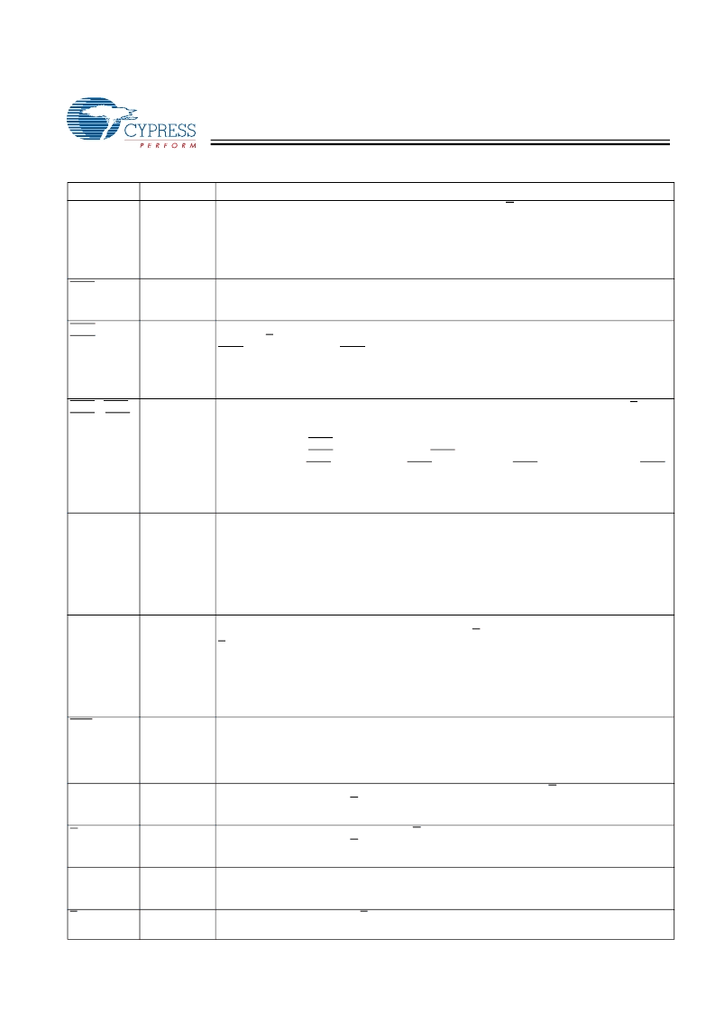
Pin Definitions
Pin Name
D
[x:0]
I/O
Pin Description
Input-
Synchronous
Data input signals, sampled on the rising edge of K and K clocks during valid write
operations
.
CY7C1411AV18
D
[7:0]
CY7C1426AV18
D
[8:0]
CY7C1413AV18
D
[17:0]
CY7C1415AV18
D
[35:0]
Write Port Select, active LOW
. Sampled on the rising edge of the K clock. When asserted active,
a Write operation is initiated. Deasserting will deselect the Write port. Deselecting the Write port
will cause D
[x:0]
to be ignored.
Nibble Write Select 0, 1
active LOW
.(CY7C1411AV18
Only
) Sampled on the rising edge of
the K and K clocks during Write operations. Used to select which nibble is written into the device
NWS
0
controls D
[3:0]
and NWS
1
controls D
[7:4]
.
All the Nibble Write Selects are sampled on the same edge as the data. Deselecting a Nibble
Write Select will cause the corresponding nibble of data to be ignored and not written into the
device.
WPS
Input-
Synchronous
NWS
0
,
NWS
1
,
Input-
Synchronous
BWS
0
, BWS
1
,
BWS
2
, BWS
3
Input-
Synchronous
Byte Write Select 0, 1, 2, and 3
active LOW
. Sampled on the rising edge of the K and K clocks
during Write operations. Used to select which byte is written into the device during the current
portion of the Write operations. Bytes not written remain unaltered.
CY7C1426AV18
BWS
0
controls D
[8:0]
CY7C1413AV18
BWS
0
controls D
[8:0]
and BWS
1
controls D
[17:9].
CY7C1415AV18
BWS
0
controls D
[8:0]
, BWS
1
controls D
[17:9]
, BWS
2
controls D
[26:18]
and BWS
3
controls D
[35:27].
All the Byte Write Selects are sampled on the same edge as the data. Deselecting a Byte Write
Select will cause the corresponding byte of data to be ignored and not written into the device.
Address Inputs
. Sampled on the rising edge of the K clock during active Read and Write opera-
tions. These address inputs are multiplexed for both Read and Write operations. Internally, the
device is organized as 4M x 8 (4 arrays each of 1M x 8) for CY7C1411AV18, 4M x 9 (4 arrays
each of 1M x 9) for CY7C1426AV18,2M x 18 (4 arrays each of 512K x 18) for CY7C1413AV18
and 1M x 36 (4 arrays each of 256K x 36) for CY7C1415AV18. Therefore, only 20 address inputs
are needed to access the entire memory array of CY7C1411AV18 and CY7C1426AV18, 19
address inputs for CY7C1413AV18 and 18 address inputs for CY7C1415AV18. These inputs are
ignored when the appropriate port is deselected.
Data Output signals
. These pins drive out the requested data during a Read operation. Valid
data is driven out on the rising edge of both the C and C clocks during Read operations or K and
K. when in single clock mode. When the Read port is deselected, Q
[x:0]
are automatically
tri-stated.
CY7C1411AV18
Q
[7:0]
CY7C1426AV18
Q
[8:0]
CY7C1413AV18
Q
[17:0]
CY7C1415AV18
Q
[35:0]
Read Port Select, active LOW
. Sampled on the rising edge of Positive Input Clock (K). When
active, a Read operation is initiated. Deasserting will cause the Read port to be deselected. When
deselected, the pending access is allowed to complete and the output drivers are automatically
tri-stated following the next rising edge of the C clock. Each Read access consists of a burst of
four sequential transfers.
Positive Input Clock for Output Data
. C is used in conjunction with C to clock out the Read
data from the device. C and C can be used together to deskew the flight times of various devices
on the board back to the controller. See application example for further details.
Negative Input Clock for Output Data
. C is used in conjunction with C to clock out the Read
data from the device. C and C can be used together to deskew the flight times of various devices
on the board back to the controller. See application example for further details.
Positive Input Clock Input
. The rising edge of K is used to capture synchronous inputs to the
device and to drive out data through Q
[x:0]
when in single clock mode. All accesses are initiated
on the rising edge of K.
Negative Input Clock Input
. K is used to capture synchronous inputs being presented to the
device and to drive out data through Q
[x:0]
when in single clock mode.
A
Input-
Synchronous
Q
[x:0]
Outputs-
Synchronous
RPS
Input-
Synchronous
C
Input-
Clock
C
Input-
Clock
K
Input-
Clock
K
Input-
Clock
[+] Feedback
相關(guān)PDF資料 |
PDF描述 |
|---|---|
| CY7C1413AV18-200BZI | 36-Mbit QDR⑩-II SRAM 4-Word Burst Architecture |
| CY7C1413AV18-200BZXC | 36-Mbit QDR⑩-II SRAM 4-Word Burst Architecture |
| CY7C1413AV18-200BZXI | 36-Mbit QDR⑩-II SRAM 4-Word Burst Architecture |
| CY7C1413AV18-250BZC | 36-Mbit QDR⑩-II SRAM 4-Word Burst Architecture |
| CY7C1413AV18-250BZI | 36-Mbit QDR⑩-II SRAM 4-Word Burst Architecture |
相關(guān)代理商/技術(shù)參數(shù) |
參數(shù)描述 |
|---|---|
| CY7C1413AV18-200BZCES | 制造商:Cypress Semiconductor 功能描述:SRAM SYNC DUAL 1.8V 36MBIT 2MX18 0.45NS 165FBGA - Bulk |
| CY7C1413AV18-200BZI | 功能描述:靜態(tài)隨機(jī)存取存儲(chǔ)器 2Mx18 QDR II Burst 4 靜態(tài)隨機(jī)存取存儲(chǔ)器 RoHS:否 制造商:Cypress Semiconductor 存儲(chǔ)容量:16 Mbit 組織:1 M x 16 訪問時(shí)間:55 ns 電源電壓-最大:3.6 V 電源電壓-最小:2.2 V 最大工作電流:22 uA 最大工作溫度:+ 85 C 最小工作溫度:- 40 C 安裝風(fēng)格:SMD/SMT 封裝 / 箱體:TSOP-48 封裝:Tray |
| CY7C1413AV18-250BZC | 功能描述:靜態(tài)隨機(jī)存取存儲(chǔ)器 2Mx18 QDR II Burst 4 靜態(tài)隨機(jī)存取存儲(chǔ)器 COM RoHS:否 制造商:Cypress Semiconductor 存儲(chǔ)容量:16 Mbit 組織:1 M x 16 訪問時(shí)間:55 ns 電源電壓-最大:3.6 V 電源電壓-最小:2.2 V 最大工作電流:22 uA 最大工作溫度:+ 85 C 最小工作溫度:- 40 C 安裝風(fēng)格:SMD/SMT 封裝 / 箱體:TSOP-48 封裝:Tray |
| CY7C1413AV18-250BZCES | 制造商:Cypress Semiconductor 功能描述:SRAM SYNC DUAL 1.8V 36MBIT 2MX18 0.45NS 165FBGA - Bulk |
| CY7C1413AV18-250BZCT | 功能描述:靜態(tài)隨機(jī)存取存儲(chǔ)器 2Mx18 QDR II Burst 4 靜態(tài)隨機(jī)存取存儲(chǔ)器 COM RoHS:否 制造商:Cypress Semiconductor 存儲(chǔ)容量:16 Mbit 組織:1 M x 16 訪問時(shí)間:55 ns 電源電壓-最大:3.6 V 電源電壓-最小:2.2 V 最大工作電流:22 uA 最大工作溫度:+ 85 C 最小工作溫度:- 40 C 安裝風(fēng)格:SMD/SMT 封裝 / 箱體:TSOP-48 封裝:Tray |
發(fā)布緊急采購(gòu),3分鐘左右您將得到回復(fù)。