- 您現(xiàn)在的位置:買賣IC網(wǎng) > PDF目錄378507 > CY7C1463AV33 (Cypress Semiconductor Corp.) 36-Mbit (1M x 36/2 M x 18/512K x 72) Flow-Through SRAM with NoBL Architecture(帶NoBL結(jié)構(gòu)的36-Mbit (1M x 36/2 M x 18/512K x 72) Flow-Through SRAM) PDF資料下載
參數(shù)資料
| 型號(hào): | CY7C1463AV33 |
| 廠商: | Cypress Semiconductor Corp. |
| 英文描述: | 36-Mbit (1M x 36/2 M x 18/512K x 72) Flow-Through SRAM with NoBL Architecture(帶NoBL結(jié)構(gòu)的36-Mbit (1M x 36/2 M x 18/512K x 72) Flow-Through SRAM) |
| 中文描述: | 36兆位(1米x 36 / 2 M中的x 18/512K × 72)流體系結(jié)構(gòu),通過與總線延遲(帶總線延遲結(jié)構(gòu)的的36 - Mbit通過的SRAM(100萬x 36 / 2 M中的x 18/512K × 72)流的SRAM ) |
| 文件頁數(shù): | 15/31頁 |
| 文件大?。?/td> | 1141K |
| 代理商: | CY7C1463AV33 |
第1頁第2頁第3頁第4頁第5頁第6頁第7頁第8頁第9頁第10頁第11頁第12頁第13頁第14頁當(dāng)前第15頁第16頁第17頁第18頁第19頁第20頁第21頁第22頁第23頁第24頁第25頁第26頁第27頁第28頁第29頁第30頁第31頁
CY7C1461AV33
CY7C1463AV33
CY7C1465AV33
Document #: 38-05356 Rev. *F
Page 15 of 31
EXTEST OUTPUT BUS TRI-STATE
IEEE Standard 1149.1 mandates that the TAP controller be
able to put the output bus into a tri-state mode.
The boundary scan register has a special bit located at bit #89
(for 165-FBGA package) or bit #138 (for 209 FBGA package).
When this scan cell, called the “extest output bus tri-state”, is
latched into the preload register during the “Update-DR” state
in the TAP controller, it directly controls the state of the output
(Q-bus) pins, when the EXTEST is entered as the current
instruction. When HIGH, it enables the output buffers to drive
the output bus. When LOW, this bit places the output bus into
a High-Z condition.
This bit can be set by entering the SAMPLE/PRELOAD or
EXTEST command, and then shifting the desired bit into that
cell, during the “Shift-DR” state. During “Update-DR”, the value
loaded into that shift-register cell latches into the preload
register. When the EXTEST instruction is entered, this bit
directly controls the output Q-bus pins. Note that this bit is
pre-set HIGH to enable the output when the device is
powered-up, and also when the TAP controller is in the
“Test-Logic-Reset” state.
Reserved
These instructions are not implemented but are reserved for
future use. Do not use these instructions.
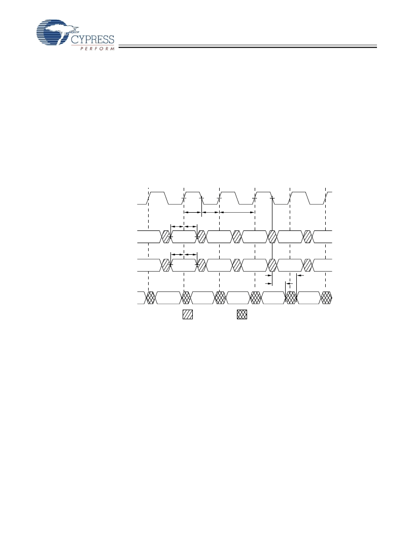
TAP Timing
tTL
Test Clock
(TCK)
1
2
3
4
5
6
Test Mode Select
(TMS)
tTH
Test Data-Out
(TDO)
tCYC
Test Data-In
(TDI)
tTMSH
tTMSS
tTDIH
tTDIS
tTDOX
tTDOV
DON’T CARE
UNDEFINED
相關(guān)PDF資料 |
PDF描述 |
|---|---|
| CY7C1465AV33 | 36-Mbit (1M x 36/2 M x 18/512K x 72) Flow-Through SRAM with NoBL Architecture(帶NoBL結(jié)構(gòu)的36-Mbit (1M x 36/2 M x 18/512K x 72) Flow-Through SRAM) |
| CY7C1470V25-250BZXC | ECONOLINE: RQS & RQD - 1kVDC Isolation- Internal SMD Construction- UL94V-0 Package Material- Toroidal Magnetics- Efficiency to 80% |
| CY7C1470V25-167AXC | 72-Mbit(2M x 36/4M x 18/1M x 72) Pipelined SRAM with NoBL⑩ Architecture |
| CY7C1470V33-167AXC | 72-Mbit (2M x 36/4M x 18/1M x 72) Pipelined SRAM with NoBL Architecture |
| CY7C1470V33-250BZXC | ECONOLINE: RQS & RQD - 1kVDC Isolation- Internal SMD Construction- UL94V-0 Package Material- Toroidal Magnetics- Efficiency to 80% |
相關(guān)代理商/技術(shù)參數(shù) |
參數(shù)描述 |
|---|---|
| CY7C1463AV33-117AXC | 功能描述:靜態(tài)隨機(jī)存取存儲(chǔ)器 2Mx18 3.3V NoBL FT 靜態(tài)隨機(jī)存取存儲(chǔ)器 COM RoHS:否 制造商:Cypress Semiconductor 存儲(chǔ)容量:16 Mbit 組織:1 M x 16 訪問時(shí)間:55 ns 電源電壓-最大:3.6 V 電源電壓-最小:2.2 V 最大工作電流:22 uA 最大工作溫度:+ 85 C 最小工作溫度:- 40 C 安裝風(fēng)格:SMD/SMT 封裝 / 箱體:TSOP-48 封裝:Tray |
| CY7C1463AV33-133AXC | 功能描述:靜態(tài)隨機(jī)存取存儲(chǔ)器 2Mx18 3.3V NoBL FT 靜態(tài)隨機(jī)存取存儲(chǔ)器 RoHS:否 制造商:Cypress Semiconductor 存儲(chǔ)容量:16 Mbit 組織:1 M x 16 訪問時(shí)間:55 ns 電源電壓-最大:3.6 V 電源電壓-最小:2.2 V 最大工作電流:22 uA 最大工作溫度:+ 85 C 最小工作溫度:- 40 C 安裝風(fēng)格:SMD/SMT 封裝 / 箱體:TSOP-48 封裝:Tray |
| CY7C1463AV33-133AXI | 功能描述:靜態(tài)隨機(jī)存取存儲(chǔ)器 2Mx18 3.3V NoBL-FT 靜態(tài)隨機(jī)存取存儲(chǔ)器 RoHS:否 制造商:Cypress Semiconductor 存儲(chǔ)容量:16 Mbit 組織:1 M x 16 訪問時(shí)間:55 ns 電源電壓-最大:3.6 V 電源電壓-最小:2.2 V 最大工作電流:22 uA 最大工作溫度:+ 85 C 最小工作溫度:- 40 C 安裝風(fēng)格:SMD/SMT 封裝 / 箱體:TSOP-48 封裝:Tray |
| CY7C1463AV33-133CKJ | 制造商:Cypress Semiconductor 功能描述: |
| CY7C1463BV33-133AXI | 功能描述:靜態(tài)隨機(jī)存取存儲(chǔ)器 36Mb (2 M x 18) 靜態(tài)隨機(jī)存取存儲(chǔ)器 靜態(tài)隨機(jī)存取存儲(chǔ)器 RoHS:否 制造商:Cypress Semiconductor 存儲(chǔ)容量:16 Mbit 組織:1 M x 16 訪問時(shí)間:55 ns 電源電壓-最大:3.6 V 電源電壓-最小:2.2 V 最大工作電流:22 uA 最大工作溫度:+ 85 C 最小工作溫度:- 40 C 安裝風(fēng)格:SMD/SMT 封裝 / 箱體:TSOP-48 封裝:Tray |
發(fā)布緊急采購(gòu),3分鐘左右您將得到回復(fù)。