- 您現(xiàn)在的位置:買賣IC網(wǎng) > PDF目錄170347 > CYW2330ZITR (CYPRESS SEMICONDUCTOR CORP) PLL FREQUENCY SYNTHESIZER, 2500 MHz, PDSO20 PDF資料下載
參數(shù)資料
| 型號(hào): | CYW2330ZITR |
| 廠商: | CYPRESS SEMICONDUCTOR CORP |
| 元件分類: | PLL合成/DDS/VCOs |
| 英文描述: | PLL FREQUENCY SYNTHESIZER, 2500 MHz, PDSO20 |
| 封裝: | 0.173 INCH, TSSOP-20 |
| 文件頁數(shù): | 6/13頁 |
| 文件大?。?/td> | 228K |
| 代理商: | CYW2330ZITR |
CYW2330
PRELIMINARY
Document #: 38-07239 Rev. **
Page 2 of 13
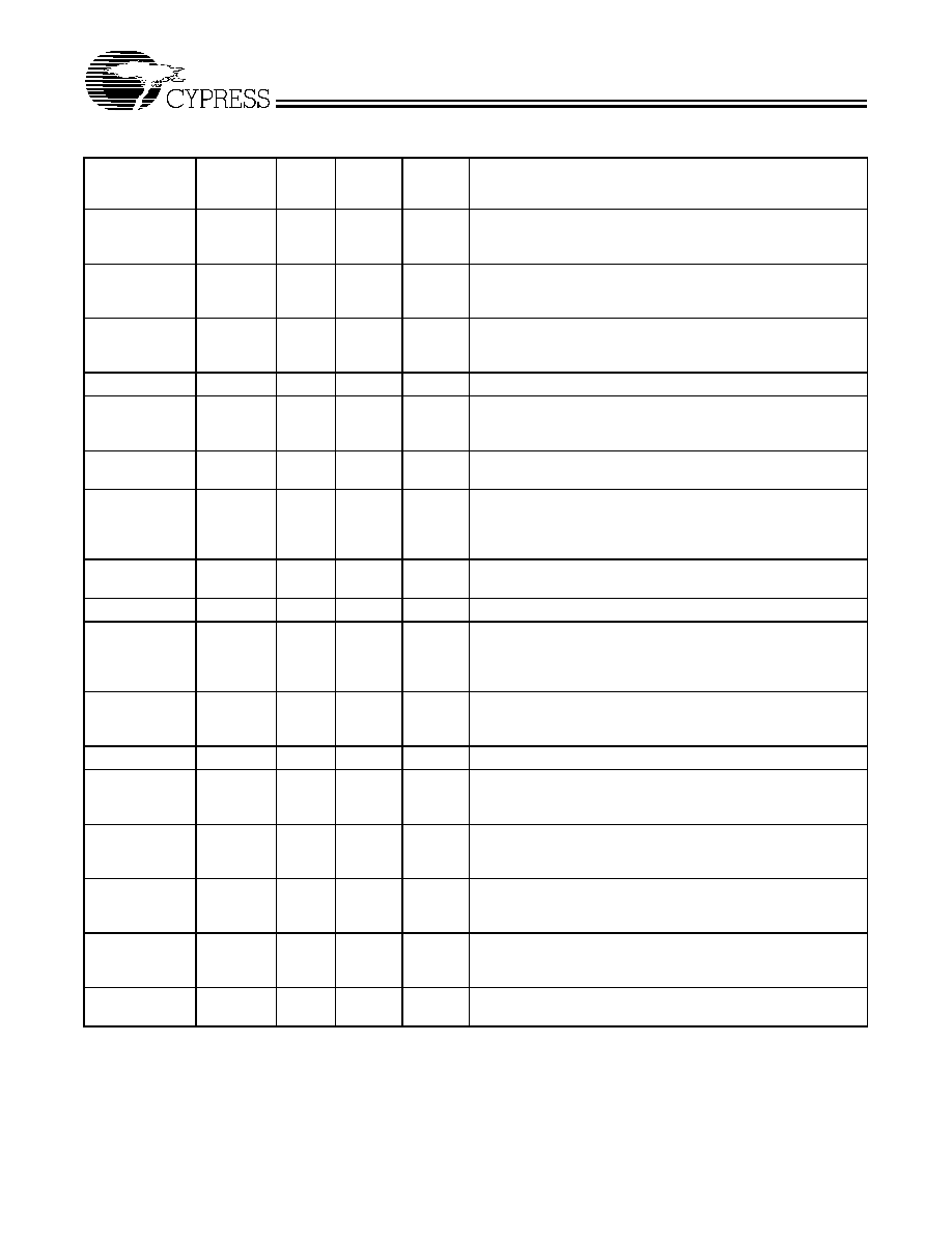
Pin Definitions
Pin Name
Pin
No.
(TSSOP)
Pin
No.
(CSP)
Pin
No.
(MLF)
Pin
Type
Pin Description
VCC1
1
24
19
P
Power Supply Connection for PLL1 and PLL2: When power
is removed from both the VCC1 and VCC2 pins, all latched data
is lost.
VP12
2
20
P
PLL1 Charge Pump Rail Voltage: This voltage accommo-
dates VCO circuits with tuning voltages higher than the VCC of
PLL1.
DOPLL1
3
1
O
PLL1 Charge Pump Output: The phase detector gain is IP/2π.
Sense polarity can be reversed by setting the FC bit in software
(via the Shift Register).
FIN15
5
3
I
Input to PLL1 Prescaler: Maximum frequency 2.5 GHz.
FIN1#
6
4
I
Complementary Input to PLL1 Prescaler: A bypass capaci-
tor should be placed as close as possible to this pin and must
be connected directly to the ground plane.
OSC_IN
8
6
I
Oscillator Input: This input has a VCC/2 threshold and CMOS
logic level sensitivity.
FO/LD
10
11
8
O
Lock Detect Pin of PLL1 Section: This output is HIGH when
the loop is locked. It is multiplexed to the output of the program-
mable counters or reference dividers in the test program mode.
(Refer to Table 3 for configuration.)
CLOCK
11
12
9
I
Data Clock Input: One bit of data is loaded into the Shift Reg-
ister on the rising edge of this signal.
DATA
12
14
10
I
Serial Data Input
LE
13
15
11
I
Load Enable: On the rising edge of this signal, the data stored
in the Shift Register is latched into the reference counter and
configuration controls, PLL1 or PLL2 depending on the state
of the control bits.
FIN2#
15
17
13
I
Complementary Input to PLL2 Prescaler: A bypass capaci-
tor should be placed as close as possible to this pin and must
be connected directly to the ground plane.
FIN216
18
14
I
Input to PLL2 Prescaler: Maximum frequency 600 MHz.
DOPLL2
18
20
16
O
PLL2 Charge Pump Output: The phase detector gain is IP/2π.
Sense polarity can be reversed by setting the FC bit in software
(via the Shift Register).
VP219
22
17
P
PLL2 Charge Pump Rail Voltage: This voltage accommo-
dates VCO circuits with tuning voltages higher than the VCC of
PLL2.
VCC220
23
18
P
Power Supply Connections for PLL1 and PLL2: When pow-
er is removed from both the VCC1 and VCC2 pins, all latched
data is lost.
GND
4, 7, 9,
14, 17
4, 7,
10,
16, 19
2, 5, 7,
12, 15
G
Analog and Digital Ground Connections: This pin must be
grounded.
N/C
N/A
1, 9,
13, 21
N/A
N/C
No Connect.
相關(guān)PDF資料 |
PDF描述 |
|---|---|
| CYW311OXCT | 200 MHz, PROC SPECIFIC CLOCK GENERATOR, PDSO48 |
| CZ23EH-FREQ-OUT23 | VCXO, CLOCK, 1.25 MHz - 65 MHz, CMOS/TTL OUTPUT |
| CZM4-2000 | VCO, 1950 MHz - 2800 MHz |
| CZSH5-40C | 2.5 A, 40 V, SILICON, RECTIFIER DIODE |
| D-20C | 8 FUNCTIONS, 50 V, 0.5 A, DATA LINE FILTER |
相關(guān)代理商/技術(shù)參數(shù) |
參數(shù)描述 |
|---|---|
| CYW2331 | 制造商:CYPRESS 制造商全稱:Cypress Semiconductor 功能描述:Dual Serial Input PLL with 2.0-GHz and 600-MHz Prescalers |
| CYW2338 | 制造商:CYPRESS 制造商全稱:Cypress Semiconductor 功能描述:Dual Serial Input PLL with 2.5- and 1.1-GHz Prescalers |
| CYW2338ZI | 制造商:Cypress Semiconductor 功能描述: |
| CYW2338ZIT | 制造商:Cypress Semiconductor 功能描述: |
| CYW255OXC | 功能描述:時(shí)鐘緩沖器 200MhZ-24 Out Buff 4 DDR3 SDRAM DIMMS RoHS:否 制造商:Texas Instruments 輸出端數(shù)量:5 最大輸入頻率:40 MHz 傳播延遲(最大值): 電源電壓-最大:3.45 V 電源電壓-最小:2.375 V 最大功率耗散: 最大工作溫度:+ 85 C 最小工作溫度:- 40 C 封裝 / 箱體:LLP-24 封裝:Reel |
發(fā)布緊急采購,3分鐘左右您將得到回復(fù)。