- 您現(xiàn)在的位置:買賣IC網(wǎng) > PDF目錄376561 > DAC7800 Dual Monolithic CMOS 12-Bit Multiplying DIGITAL-TO-ANALOG CONVERTERS PDF資料下載
參數(shù)資料
| 型號(hào): | DAC7800 |
| 英文描述: | Dual Monolithic CMOS 12-Bit Multiplying DIGITAL-TO-ANALOG CONVERTERS |
| 中文描述: | 雙路單片CMOS 12位乘法數(shù)字到模擬轉(zhuǎn)換器 |
| 文件頁(yè)數(shù): | 8/12頁(yè) |
| 文件大?。?/td> | 180K |
| 代理商: | DAC7800 |

8
DAC7800, 01, 02
DISCUSSION OF
SPECIFICATIONS
RELATIVE ACCURACY
This term, also known as end point linearity or integral
linearity, describes the transfer function of analog output to
digital input code. Relative accuracy describes the deviation
from a straight line, after zero and full scale errors have been
adjusted to zero.
DIFFERENTIAL NONLINEARITY
Differential nonlinearity is the deviation from an ideal 1LSB
change in the output when the input code changes by 1LSB.
A differential nonlinearity specification of 1LSB maximum
guarantees monotonicity.
GAIN ERROR
Gain error is the difference between the full-scale DAC
output and the ideal value. The ideal full scale output value
for the DAC780X is –(4095/4096)V
REF
. Gain error may be
adjusted to zero using external trims as shown in Figures 5
and 7.
OUTPUT LEAKAGE CURRENT
The current which appears at I
OUT A
and I
OUT B
with the DAC
loaded with all zeros.
OUTPUT CAPACITANCE
The parasitic capacitance measured from I
OUT A
or I
OUT B
to
AGND.
CHANNEL-TO-CHANNEL ISOLATION
The AC output error due to capacitive coupling from DAC A
to DAC B or DAC B to DAC A.
MULTIPLYING FEEDTHROUGH ERROR
The AC output error due to capacitive coupling from V
REF
to
I
OUT
with the DAC loaded with all zeros.
OUTPUT CURRENT SETTLING TIME
The time required for the output current to settle to within
+0.01% of final value for a full scale step.
DIGITAL-TO-ANALOG GLITCH ENERGY
The integrated area of the glitch pulse measured in nanovolt-
seconds. The key contributor to digital-to-analog glitch is
charge injected by digital logic switching transients.
DIGITAL CROSSTALK
Glitch impulse measured at the output of one DAC but
caused by a full scale transition on the other DAC. The
integrated area of the glitch pulse is measured in nanovolt-
seconds.
CIRCUIT DESCRIPTION
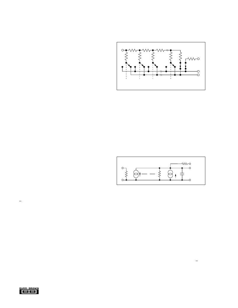
Figure 1 shows a simplified schematic of one half of a
DAC780X. The current from the V
REF
A
pin is switched
between I
OUT A
and AGND by 12 single-pole double-throw
CMOS switches. This maintains a constant current in each leg
A CMOS switch transistor, included in series with the ladder
terminating resistor and in series with the feedback resistor,
R
FB A
, compensates for the temperature drift of the ON
resistance of the ladder switches.
Figure 2 shows an equivalent circuit for DAC A. C
OUT
is the
output capacitance due to the N-channel switches and varies
from about 30pF to 70pF with digital input code. The current
source I
LKG
is the combination of surface and junction leak-
ages to the substrate. I
LKG
approximately doubles every 10
°
C.
R
O
is the equivalent output resistance of the D/A and it varies
with input code.
of the ladder regardless of the input code. The input resistance
at V
REF
is therefore constant and can be driven by either a
voltage or current, AC or DC, positive or negative polarity,
and have a voltage range up to
±
20V.
OUT A
I
AGND
FB A
R
2R
2R
2R
2R
2R
R
R
R
V
REF A
DB11
(MSB)
DB10
DB9
DB0
(LSB)
R
FIGURE 1. Simplified Circuit Diagram for DAC A.
FIGURE 2. Equivalent Circuit for DAC A.
FB A
R
I
OUT A
V
REF A
I
LKG
R
OUT
C
O
R
AGND A
D
IN
4096
x
V
REF
R
R
INSTALLATION
ESD PROTECTION
All digital inputs of the DAC780X incorporate on-chip ESD
protection circuitry. This protection is designed to withstand
2.5kV (using the Human Body Model, 100pF and 1500
).
However, industry standard ESD protection methods should
be used when handling or storing these components. When
not in use, devices should be stored in conductive foam or
rails. The foam or rails should be discharged to the destina-
tion socket potential before devices are removed.
POWER SUPPLY CONNECTIONS
The DAC780X are designed to operate on V
DD
= +5V +10%.
For optimum performance and noise rejection, power supply
decoupling capacitors C
D
should be added as shown in the
application circuits. These capacitors (1
μ
F tantalum recom-
mended) should be located close to the D/A. AGND and
相關(guān)PDF資料 |
PDF描述 |
|---|---|
| DAC7801 | Dual Monolithic CMOS 12-Bit Multiplying DIGITAL-TO-ANALOG CONVERTERS |
| DAC7802L | Dual Monolithic CMOS 12-Bit Multiplying DIGITAL-TO-ANALOG CONVERTERS |
| DAC7811IDRCT | 12-Bit, Serial Input, Multiplying Digital-to-Analog Converter |
| DAC7811IDRCR | 12-Bit, Serial Input, Multiplying Digital-to-Analog Converter |
| DAC7821IRGPR | 50/MDR/WMNT/PLASTIC PLUG/20MIN |
相關(guān)代理商/技術(shù)參數(shù) |
參數(shù)描述 |
|---|---|
| DAC7800/DAC7801/DAC7802 | 制造商:BB 制造商全稱:BB 功能描述:DAC7800. DAC7801. DAC7802 - Dual Monolithic CMOS 12-Bit Multiplying DIGITAL-TO-ANALOG CONVERTERS |
| DAC7800_04 | 制造商:BB 制造商全稱:BB 功能描述:Dual Monolithic CMOS 12-Bit Multiplying DIGITAL-TO-ANALOG CONVERTERS |
| DAC7800KP | 功能描述:數(shù)模轉(zhuǎn)換器- DAC Dual Monolithic CMOS 12-Bit Multiplying RoHS:否 制造商:Texas Instruments 轉(zhuǎn)換器數(shù)量:1 DAC 輸出端數(shù)量:1 轉(zhuǎn)換速率:2 MSPs 分辨率:16 bit 接口類型:QSPI, SPI, Serial (3-Wire, Microwire) 穩(wěn)定時(shí)間:1 us 最大工作溫度:+ 85 C 安裝風(fēng)格:SMD/SMT 封裝 / 箱體:SOIC-14 封裝:Tube |
| DAC7800KP | 制造商:Texas Instruments 功能描述:Digital/Analog Converter IC Interface Ty |
| DAC7800KPG4 | 功能描述:數(shù)模轉(zhuǎn)換器- DAC Dual Monolithic CMOS 12-Bit Multiplying RoHS:否 制造商:Texas Instruments 轉(zhuǎn)換器數(shù)量:1 DAC 輸出端數(shù)量:1 轉(zhuǎn)換速率:2 MSPs 分辨率:16 bit 接口類型:QSPI, SPI, Serial (3-Wire, Microwire) 穩(wěn)定時(shí)間:1 us 最大工作溫度:+ 85 C 安裝風(fēng)格:SMD/SMT 封裝 / 箱體:SOIC-14 封裝:Tube |
發(fā)布緊急采購(gòu),3分鐘左右您將得到回復(fù)。