- 您現(xiàn)在的位置:買賣IC網(wǎng) > PDF目錄376562 > DAC811AH Microprocessor-Compatible 12-BIT DIGITAL-TO-ANALOG CONVERTER PDF資料下載
參數(shù)資料
| 型號: | DAC811AH |
| 英文描述: | Microprocessor-Compatible 12-BIT DIGITAL-TO-ANALOG CONVERTER |
| 中文描述: | 微處理器兼容的12位數(shù)字到模擬轉(zhuǎn)換器 |
| 文件頁數(shù): | 7/9頁 |
| 文件大?。?/td> | 96K |
| 代理商: | DAC811AH |

7
DAC811
DAC811 features separate digital and analog power supply
returns to permit optimum connections for low noise and
high speed performance. The analog common (pin 23) and
digital common (pin 15) should be connected together at one
point. Separate returns minimize current flow in low level
signal paths if properly connected. Logic return currents are
not added into the analog signal return path. A
±
0.5V
difference between ACOM and DCOM is permitted for
specified operation. High frequency noise on DCOM with
respect to ACOM may permit noise to be coupled through to
the analog output; therefore, some caution is required in
applying these common connections.
The Analog Common is the high quality return for the D/A
converter and should be connected directly to the analog
reference point of the system. The load driven by the output
amplifier should be returned to the Analog Common.
EXTERNAL OFFSET AND GAIN ADJUSTMENT
Offset and Gain may be trimmed by installing external
Offset and Gain potentiometers. Connect these potentiom-
eters as shown in Figure 5. TCR of the potentiometers
should be 100ppm/
°
C or less. The 1M
and 3.9M
resis-
tors (20% carbon or better) should be located close to the
DAC811 to prevent noise pickup. If it is not convenient to
use these high value resistors, an equivalent “T” network, as
shown in Figure 6, may be substituted in each case. The
Gain Adjust (pin 22) is a high impedance point and a
0.001
μ
F to 0.01
μ
F ceramic capacitor should be connected
from this pin to Analog Common to reduce noise pickup in
all applications, including those not employing external gain
adjustment. Excessive capacitance on the Gain Adjust or
Offset Adjust pin may affect slew rate and settling time.
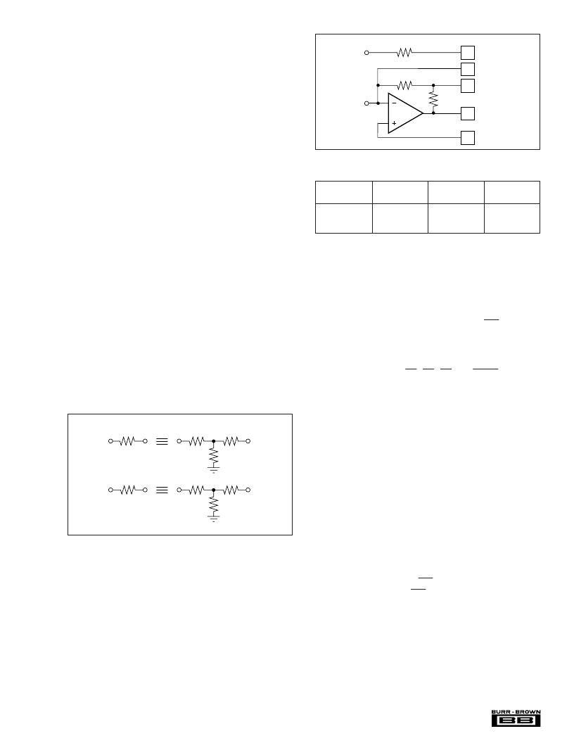
FIGURE 6. Equivalent Resistances.
FIGURE 7. Output Amplifier Voltage Range Scaling Circuit.
OUTPUT
RANGE
DIGITAL
INPUT CODES
CONNECT
PIN 25 TO
CONNECT
PIN 27 TO
0 to +10V
±
5
±
10V
USB
24
24
NC
23
26
26
BOB or BTC
BOB or BTC
TABLE IV. Output Range Connections.
APPLICATIONS
MICROCOMPUTER BUS INTERFACING
The DAC811 interface logic allows easy interface to micro-
computer bus structures. The control signal WR is derived
from external device select logic and the I/O Write or
Memory Write (depending upon the system design) signals
from the microcomputer.
The latch enable lines N
A
, N
B
, N
C
and LDAC determine
which of the latches are enabled. It is permissible to enable
two or more latches simultaneously, as shown in some of the
following examples.
The double-buffered latch permits data to be loaded into the
input latches of several DAC811s and later strobed into the
D/A latch of all D/As, simultaneously updating all analog
outputs. All the interface schemes shown below use a base
address decoder. If blocks of memory are used, the base
address decoder can be simplified or eliminated altogether.
For instance, if half the memory space is unused, address
line A15 of the microcomputer can be used as the chip select
control.
4-BIT INTERFACE
An interface to a 4-bit microcomputer is shown in Figure 8.
Each DAC811 occupies four address locations. A 74LS139
provides the two-to-four decoder and selects it with the base
address. Memory Write (WR) of the microcomputer is
connected directly to the WR pin of the DAC811. An 8205
decoder is an alternative to the 74LS139.
OUTPUT RANGE CONNECTIONS
Internal scaling resistors provided in the DAC811 may be
connected to produce bipolar output voltage ranges of
±
10V
and
±
5V or a unipolar output voltage range of 0 to +10V.
The 20V range (
±
10V bipolar range) is internally connected.
Refer to Figure 7. Connections for the output ranges are
listed in Table IV.
1M
3.9M
100k
100k
12k
10k
180k
180k
4.26k
5.36k
24
V
OUT
23
Analog Common
From D/A
Converter
From Voltage
Reference
4.26k
25
10V Range
26
Summing Junction
27
Bipolar Offset
相關(guān)PDF資料 |
PDF描述 |
|---|---|
| DAC811BH | Microprocessor-Compatible 12-BIT DIGITAL-TO-ANALOG CONVERTER |
| DAC811JP | Microprocessor-Compatible 12-BIT DIGITAL-TO-ANALOG CONVERTER |
| DAC811JU | Microprocessor-Compatible 12-BIT DIGITAL-TO-ANALOG CONVERTER |
| DAC811KP | Microprocessor-Compatible 12-BIT DIGITAL-TO-ANALOG CONVERTER |
| DAC811KU | Microprocessor-Compatible 12-BIT DIGITAL-TO-ANALOG CONVERTER |
相關(guān)代理商/技術(shù)參數(shù) |
參數(shù)描述 |
|---|---|
| DAC811AH | 制造商:Texas Instruments 功能描述:D/A Converter (D-A) IC |
| DAC811BH | 功能描述:數(shù)模轉(zhuǎn)換器- DAC Mcrprcsr-Compatible 12-Bit RoHS:否 制造商:Texas Instruments 轉(zhuǎn)換器數(shù)量:1 DAC 輸出端數(shù)量:1 轉(zhuǎn)換速率:2 MSPs 分辨率:16 bit 接口類型:QSPI, SPI, Serial (3-Wire, Microwire) 穩(wěn)定時間:1 us 最大工作溫度:+ 85 C 安裝風(fēng)格:SMD/SMT 封裝 / 箱體:SOIC-14 封裝:Tube |
| DAC811JP | 功能描述:數(shù)模轉(zhuǎn)換器- DAC Mcrprcsr-Compatible 12-Bit RoHS:否 制造商:Texas Instruments 轉(zhuǎn)換器數(shù)量:1 DAC 輸出端數(shù)量:1 轉(zhuǎn)換速率:2 MSPs 分辨率:16 bit 接口類型:QSPI, SPI, Serial (3-Wire, Microwire) 穩(wěn)定時間:1 us 最大工作溫度:+ 85 C 安裝風(fēng)格:SMD/SMT 封裝 / 箱體:SOIC-14 封裝:Tube |
| DAC811JPG4 | 功能描述:數(shù)模轉(zhuǎn)換器- DAC Mcrprcsr-Compatible 12-Bit RoHS:否 制造商:Texas Instruments 轉(zhuǎn)換器數(shù)量:1 DAC 輸出端數(shù)量:1 轉(zhuǎn)換速率:2 MSPs 分辨率:16 bit 接口類型:QSPI, SPI, Serial (3-Wire, Microwire) 穩(wěn)定時間:1 us 最大工作溫度:+ 85 C 安裝風(fēng)格:SMD/SMT 封裝 / 箱體:SOIC-14 封裝:Tube |
| DAC811JU | 功能描述:數(shù)模轉(zhuǎn)換器- DAC Mcrprcsr-Compatible 12-Bit RoHS:否 制造商:Texas Instruments 轉(zhuǎn)換器數(shù)量:1 DAC 輸出端數(shù)量:1 轉(zhuǎn)換速率:2 MSPs 分辨率:16 bit 接口類型:QSPI, SPI, Serial (3-Wire, Microwire) 穩(wěn)定時間:1 us 最大工作溫度:+ 85 C 安裝風(fēng)格:SMD/SMT 封裝 / 箱體:SOIC-14 封裝:Tube |
發(fā)布緊急采購,3分鐘左右您將得到回復(fù)。