- 您現(xiàn)在的位置:買賣IC網(wǎng) > PDF目錄376565 > DAC8820IB (Texas Instruments, Inc.) 16-Bit, Parallel Input Multiplying Digital-to-Analog Converter PDF資料下載
參數(shù)資料
| 型號: | DAC8820IB |
| 廠商: | Texas Instruments, Inc. |
| 英文描述: | 16-Bit, Parallel Input Multiplying Digital-to-Analog Converter |
| 中文描述: | 16位并行輸入乘法數(shù)字到模擬轉(zhuǎn)換器 |
| 文件頁數(shù): | 12/22頁 |
| 文件大小: | 939K |
| 代理商: | DAC8820IB |
www.ti.com
T
45
-
55
-
65
-
75
-
85
-
95
-
105
-
115
-
10
100
1000
10k 20k 30k
Frequency (Hz)
500kHz Filter
80kHz Filter
30kHz Filter
Code FFFFh
V
= 6V
REF
V
= +5V
DD
One OPA627
C = 20pF
RMS
THEORY OF OPERATION
R
R
R
I
OUT
GND
V
REF
2R
2R
2R
2R
2R
2R
2R
2R
2R
2R
2R
2R
R
FB
V
OUT
V
REF
D
65536
(1)
DAC8820
SBAS358C–AUGUST 2005–REVISED JUNE 2006
TYPICAL CHARACTERISTICS (continued)
At T
A
= +25
°
C, unless otherwise noted.
UNIPOLAR MULTIPLYING MODE THD
vs FREQUENCY
Figure 37.
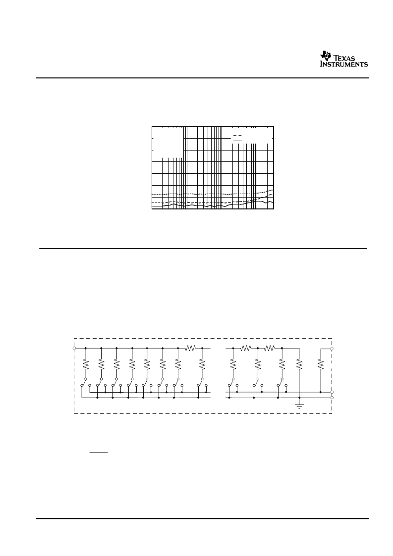
The DAC8820 is a multiplying, single-channel current output, 16-bit DAC. The architecture, illustrated in
Figure 38
, is an R-2R ladder configuration with the three MSBs segmented. Each 2R leg of the ladder is either
switched to GND or to the I
OUT
terminal. The I
OUT
terminal of the DAC is held at a virtual GND potential by the
use of an external I/V converter op amp. The R-2R ladder is connected to an external reference input (V
REF
) that
determines the DAC full-scale current. The R-2R ladder presents a code independent load impedance to the
external reference of 6 k
±
25%. The external reference voltage can vary in a range of –15 V to +15 V, thus
providing bipolar I
OUT
current operation. By using an external I/V converter op amp and the R
FB
resistor in the
DAC8820, an output voltage range of –V
REF
to +V
REF
can be generated.
Figure 38. Equivalent R-2R DAC Circuit
The DAC output voltage is determined by V
REF
and the digital data (D) according to
Equation 1
:
Each DAC code determines the 2R-leg switch position to either GND or I
OUT
. The external I/V converter op amp
noise gain will also change because the DAC output impedance (as seen looking into the I
terminal) changes
versus code. Because of this, the external I/V converter op amp must have a sufficiently low offset voltage such
that the amplifier offset is not modulated by the DAC I
OUT
terminal impedance change. External op amps with
large offset voltages can produce INL errors in the transfer function of the DAC8820 because of offset
modulation versus DAC code. For best linearity performance of the DAC8820, an op amp (OPA277) is
recommended, as shown in
Figure 39
. This circuit allows V
REF
to swing from –10 V to +10 V.
12
Submit Documentation Feedback
相關(guān)PDF資料 |
PDF描述 |
|---|---|
| DAC8820IC | 16-Bit, Parallel Input Multiplying Digital-to-Analog Converter |
| DAC8832IBRGY | 16-Bit, Ultra-Low Power, Voltage-Output Digital-to-Analog Converter |
| DAC8832ICRGY | 16-Bit, Ultra-Low Power, Voltage-Output Digital-to-Analog Converter |
| DAC8832IRGY | 16-Bit, Ultra-Low Power, Voltage-Output Digital-to-Analog Converter |
| DAC8840FP | 8-Bit Octal, 4-Quadrant Multiplying, CMOS TrimDAC |
相關(guān)代理商/技術(shù)參數(shù) |
參數(shù)描述 |
|---|---|
| DAC8820IBDB | 功能描述:數(shù)模轉(zhuǎn)換器- DAC 16-Bit Parallel Inp Multiplying DAC RoHS:否 制造商:Texas Instruments 轉(zhuǎn)換器數(shù)量:1 DAC 輸出端數(shù)量:1 轉(zhuǎn)換速率:2 MSPs 分辨率:16 bit 接口類型:QSPI, SPI, Serial (3-Wire, Microwire) 穩(wěn)定時間:1 us 最大工作溫度:+ 85 C 安裝風(fēng)格:SMD/SMT 封裝 / 箱體:SOIC-14 封裝:Tube |
| DAC8820IBDBG4 | 功能描述:數(shù)模轉(zhuǎn)換器- DAC 16-Bit Parallel Inp Multiplying DAC RoHS:否 制造商:Texas Instruments 轉(zhuǎn)換器數(shù)量:1 DAC 輸出端數(shù)量:1 轉(zhuǎn)換速率:2 MSPs 分辨率:16 bit 接口類型:QSPI, SPI, Serial (3-Wire, Microwire) 穩(wěn)定時間:1 us 最大工作溫度:+ 85 C 安裝風(fēng)格:SMD/SMT 封裝 / 箱體:SOIC-14 封裝:Tube |
| DAC8820IBDBR | 功能描述:數(shù)模轉(zhuǎn)換器- DAC 16-Bit Parallel Inp RoHS:否 制造商:Texas Instruments 轉(zhuǎn)換器數(shù)量:1 DAC 輸出端數(shù)量:1 轉(zhuǎn)換速率:2 MSPs 分辨率:16 bit 接口類型:QSPI, SPI, Serial (3-Wire, Microwire) 穩(wěn)定時間:1 us 最大工作溫度:+ 85 C 安裝風(fēng)格:SMD/SMT 封裝 / 箱體:SOIC-14 封裝:Tube |
| DAC8820IBDBRG4 | 功能描述:數(shù)模轉(zhuǎn)換器- DAC 16-Bit Parallel Inp RoHS:否 制造商:Texas Instruments 轉(zhuǎn)換器數(shù)量:1 DAC 輸出端數(shù)量:1 轉(zhuǎn)換速率:2 MSPs 分辨率:16 bit 接口類型:QSPI, SPI, Serial (3-Wire, Microwire) 穩(wěn)定時間:1 us 最大工作溫度:+ 85 C 安裝風(fēng)格:SMD/SMT 封裝 / 箱體:SOIC-14 封裝:Tube |
| DAC8820IC | 制造商:TI 制造商全稱:Texas Instruments 功能描述:16-Bit, Parallel Input Multiplying Digital-to-Analog Converter |
發(fā)布緊急采購,3分鐘左右您將得到回復(fù)。